Photoetching rework photoresist removing technology

A technology of photoresist and lithography, which is applied in the processing of photosensitive materials, electrical components, semiconductor/solid-state device manufacturing, etc., can solve the problems of wafer substrate unevenness and material, condition changes, unfavorable lithography, etc., to achieve The effect of stable secondary photolithography process, less raw material consumption, and improved stability and manufacturability

Active Publication Date: 2013-08-21
SHANGHAI HUALI MICROELECTRONICS CORP
View PDF4 Cites 12 Cited by
  • Summary
  • Abstract
  • Description
  • Claims
  • Application Information

AI Technical Summary

Problems solved by technology

Specifically, for reworked wafers, two steps are required: plasma ashing to remove glue and chemical liquid cleaning: a. The plasma ashing process will introduce highly reactive plasma and high temperature, and these plasmas will interact with the substrate of the wafer. The substance reacts to form a modified layer, resulting in a change in the conditions of the secondary photolithography, and at the same time, some photoresist or carbon-containing residues will be produced; b. For the photoresist or carbon-containing residues generated by the ashing process After cleaning with chemical liquid, these strong acidic or strong alkaline chemical liquids will etch the wafer substrate and the modified layer on the substrate, so the wafer substrate will produce uneven morphology and materials loss, which is not conducive to the subsequent lithography

Method used


Image

  • Photoetching rework photoresist removing technology
  • Photoetching rework photoresist removing technology
  • Photoetching rework photoresist removing technology

Examples


no. 1 example

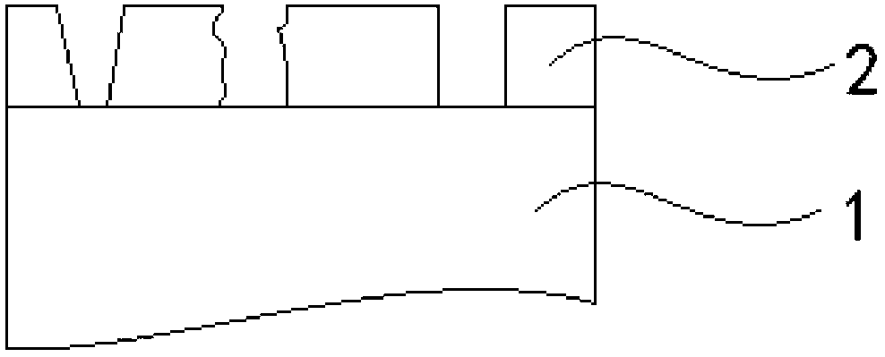
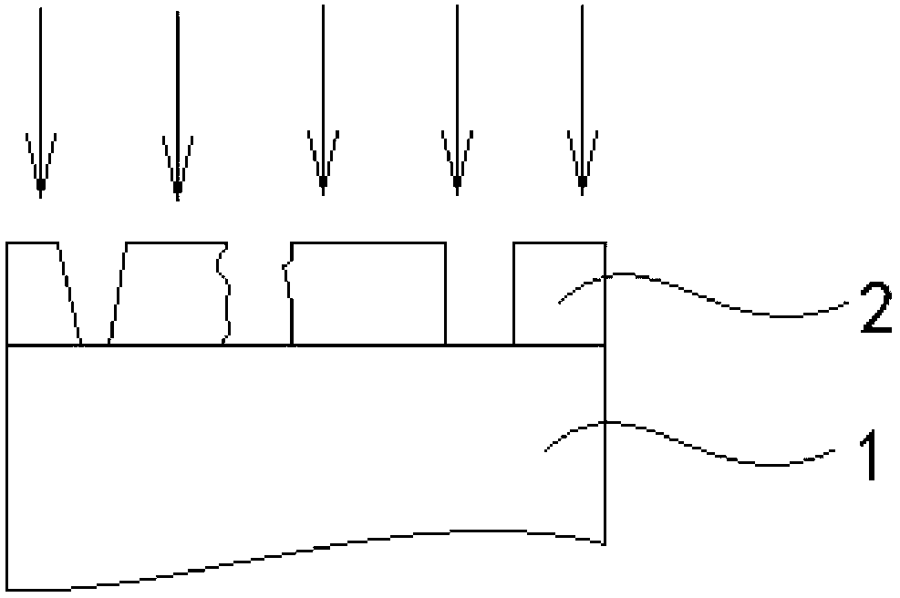
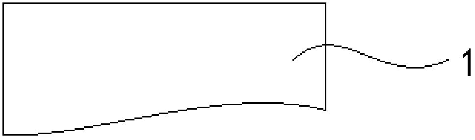
[0028] Take polysilicon gate photolithographic rework at the 40nm technology node as an example.

[0029] As we all know, the lithography of the gate layer is one of the most important steps in the manufacturing process of integrated circuit chips, and the precision requirements are also the highest. In addition, the plasma in the ashing process will cause the loss of polysilicon and the distribution of ion-implanted impurities, so it is desirable to have a low-temperature and non-destructive adhesive removal method.

[0030] see Figure 1 to Figure 3 , the wafer process process completed the preparation of the polysilicon gate layer 1 at the 40nm node, and the polysilicon gate layer needs to be photoetched. After the first photoetching was performed using argon fluoride 193 nm ultraviolet light, a poor photoetching process occurred. Resulting in unacceptable size, registration and shape of the photoresist 2-hole slot, requiring photolithographic rework to remove all photores...


PUM


Abstract

The invention discloses a photoetching rework photoresist removing technology which comprises the steps of: providing a wafer to be treated by photoetching rework; photoetching the surface of the wafer for a first time to produce residual photoresist; using a photoetching machine which can generate a light beam capable of enabling the photoresist to be in complete photochemical reaction to expose the surface of the whole wafer; and developing the surface of the exposed wafer, and removing the photoresist. According to the technology, plasma dry ashing does not need to be utilized, high-temperature manufacture procedure does not exist, and chemical liquid with strong oxidizing property or acidity is not needed, so that a film on the surface of the wafer is not damaged or modified. The technology is simple and less in material consumption, improves the stability and the manufacturing performance of the whole manufacturing process flow, and adds the limitation for the maximum photoetching rework times, thus providing high technical fault tolerance for research, development and mass production.

Description

technical field [0001] The invention relates to the field of semiconductor manufacturing, in particular to a deglue process for photolithography rework in the field of pattern photolithography technology. Background technique [0002] As an important process in the semiconductor process, the photolithography process uses a photolithography machine to transfer the pattern on the projection mask to the photoresist layer on the wafer. In order to ensure that the position and shape of the pattern formed in the photoresist layer are consistent with the position and shape on the projection mask, the photolithography machine first performs an alignment step, that is, aligning the alignment marks on the wafer with the Aligning the alignment marks on the projection mask; then, performing a focusing step, that is, adjusting the height of the wafer in the lithography machine so that the wafer is within the focus range of the optical system of the lithography machine . After the align...

Claims


Application Information

Patent Timeline
Patent Type & Authority Applications(China)
IPC IPC(8): G03F7/42H01L21/311
Inventor 张亮毛智彪
Owner SHANGHAI HUALI MICROELECTRONICS CORP
Why Eureka
Try Eureka