Method for preparing semiconductor Fe2O3 film-type surface Raman scattering substrate

A surface Raman and thin-film technology, which is applied in the field of laser Raman spectroscopy detection equipment, achieves the effect of low cost, simple preparation method and orderly distribution of surface particles

Inactive Publication Date: 2013-08-28
JIANGSU UNIV
View PDF2 Cites 4 Cited by
  • Summary
  • Abstract
  • Description
  • Claims
  • Application Information

AI Technical Summary

Problems solved by technology

[0004] Some semiconductor nanoparticles (such as ZnO, NiO and TiO2 etc. (Yamada H, et al. Surf. Sci. 1983, 134, 71 .; Wang Y X, et al. J. Raman Spectrosc. 2007, 38, 34.; Liu Y C, et al. Chem. Phys. Lett. 2006, 420, 245.)) Substrates have been studied, but they are mostly disordered However, this has certain limitations for the systematic study of its surface-enhanced Raman scattering effect; in this chapter, we successfully synthesized α-Fe2O3 nanoparticles are immobilized on the surface of the glass substrate, and form an ordered monolayer or sub-monolayer α-Fe2O3 film

Method used


Image

  • Method for preparing semiconductor Fe2O3 film-type surface Raman scattering substrate
  • Method for preparing semiconductor Fe2O3 film-type surface Raman scattering substrate
  • Method for preparing semiconductor Fe2O3 film-type surface Raman scattering substrate

Examples


Embodiment 1

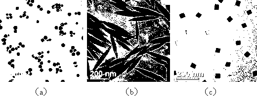
[0027] Get three kinds of α-Fe prepared by the inventive method 2 o 3 Ordered film substrates ( figure 2 : sphere, spindle shape, cube shape), the immersion concentration is 1×10 -6 M's p-mercaptopyridine (4-Mpy) methanol solution (10mL), carefully stirred with a glass rod for 0.5 hours, and allowed to stand at room temperature for 12 hours; then rinsed with methanol three times, and after the solvent on the substrate evaporated, the sample was used for Raman testing. Test results such as image 3 shown.

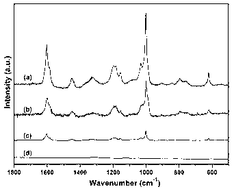
[0028] image 3 three α-Fe 2 o 3 Surface-enhanced Raman spectrum of 4-Mpy molecule adsorbed on the surface of ordered film substrate, when no film substrate is used, 1×10 -6 The 4-Mpy solution of M could not detect any Raman signal ( image 3 d); while applying thin film substrates, 1×10 -6 The enhanced Raman signal of the 4-Mpy molecule of M is very evident, in which the spherical α-Fe 2 o 3 The enhancement signal of the thin film substrate is the strongest ( im...

Embodiment 2

[0030] This embodiment selects the spherical α-Fe prepared in embodiment 1 2 o 3 Ordered film substrates were soaked in 10 mg / L aqueous solution of adenine (A), thymine (T), cytosine (C), and guanine (G) for 12 hours, then dried naturally, and the surface enhancement was measured. Raman spectrum, the test results are as follows Figure 4 shown; Figure 4 The enhanced Raman signal of A, T, C, G showing 10 mg / L in the prepared film substrate is very obvious, can pass through respective characteristic peak (947,725cm -1 ), (945,655 cm -1 ), (978,796 cm -1 ), (989,745 cm -1 ) effectively distinguishes A, T, C, and G molecules qualitatively.

Embodiment 3

[0032] This embodiment selects the spherical α-Fe prepared in embodiment 1 2 o 3 Ordered film substrates were immersed in concentrations of 1 × 10 -5 M, 1×10 -6 M, 1×10 -7 M, 1×10 -8 M, 1×10 -9 M, 1×10 -10 M, 1×10 -12 M's p-mercaptopyridine (4-Mpy) in methanol (10 mL). The glass rod was carefully stirred for 0.5 hours and allowed to stand at room temperature for 12 hours. Then rinse with methanol three times, after the solvent on the substrate evaporates, the sample is used for Raman test, the test results are as follows Figure 5 Shown: The concentration of 4-Mpy is 1 × 10 -5 M, 1×10 -6 M, 1×10 -7 M, 1×10 -8 M, its spherical α-Fe 2 o 3 The enhanced Raman signal intensity on the film substrate is almost the same; and when the concentration of 4-Mpy continues to decrease, the enhanced Raman signal intensity weakens, but the lowest detection limit can reach 1×10 -12 M, through calculation, its enhancement factor can reach up to 1.25×10 4 .


PUM

PropertyMeasurementUnit
particle diameteraaaaaaaaaa

Abstract

The invention belongs to the technical field of laser Raman spectroscopy detection equipments, and in particular relates to a method for preparing semiconductor alpha-Fe2O3 film-type surface-enhanced Raman scattering substrate. The method is characterized in that a glass substrate is immersed in an isocyanate solution for surface functionalization, and the functionalized substrate surface is modified with an alpha-Fe2O3 ordered film layer to obtain a semiconductor film substrate with a surface-enhanced Raman scattering effect. The substrate prepared by the method of the invention is order in surface particle distribution, is good in spectral signal stability, and can be used for detection and analysis of trace amounts of organic molecules, and biological molecules such as pyrimidine and purine.

Description

technical field [0001] The invention belongs to the technical field of laser Raman spectrum detection equipment, in particular to a semiconductor α-Fe 2 o 3 A method for preparing a thin-film surface-enhanced Raman scattering substrate. Background technique [0002] With the rapid development of the semiconductor nanoparticle industry, more and more people pay attention to the science and technology of semiconductor thin films. The research and development of semiconductor thin films provide a material basis for the development of emerging interdisciplinary subjects such as microelectronics, optoelectronics, and magnetoelectronics. It has become an important task to develop high-quality semiconductor thin film growth processes and to study the composition, crystal structure and physical properties of semiconductor thin films. An important part of developing these emerging disciplines. [0003] We know that the design of surface-enhanced Raman scattering substrates needs t...

Claims


Application Information

Patent Timeline
Patent Type & Authority Applications(China)
IPC IPC(8): G01N21/65
Inventor 傅小奇王双殷恒波姜廷顺
Owner JIANGSU UNIV
Why Eureka
Try Eureka