Measurement device and measurement method of optical parameters of dielectric film
A technology for dielectric thin films and optical parameters, applied in the field of optical measurement, can solve the problems of high price, complicated measurement process, and inability to measure the refractive index and thickness of dielectric thin films.
- Summary
- Abstract
- Description
- Claims
- Application Information
AI Technical Summary
Problems solved by technology
Method used
Image
Examples
Embodiment 1
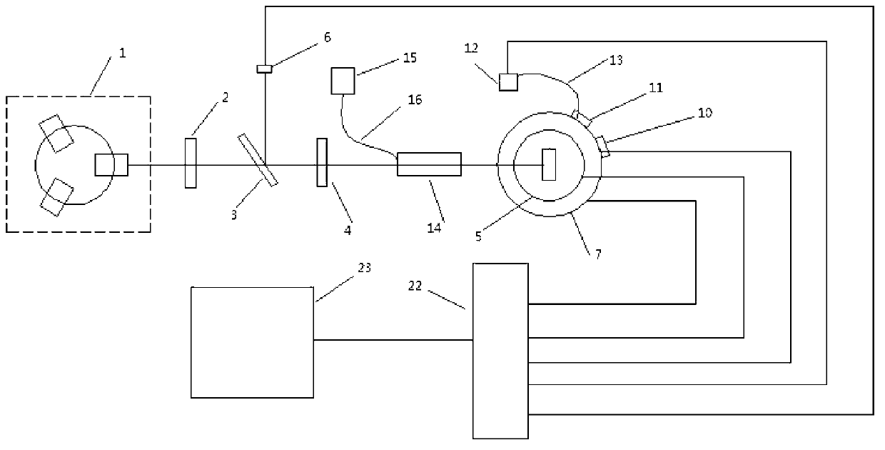
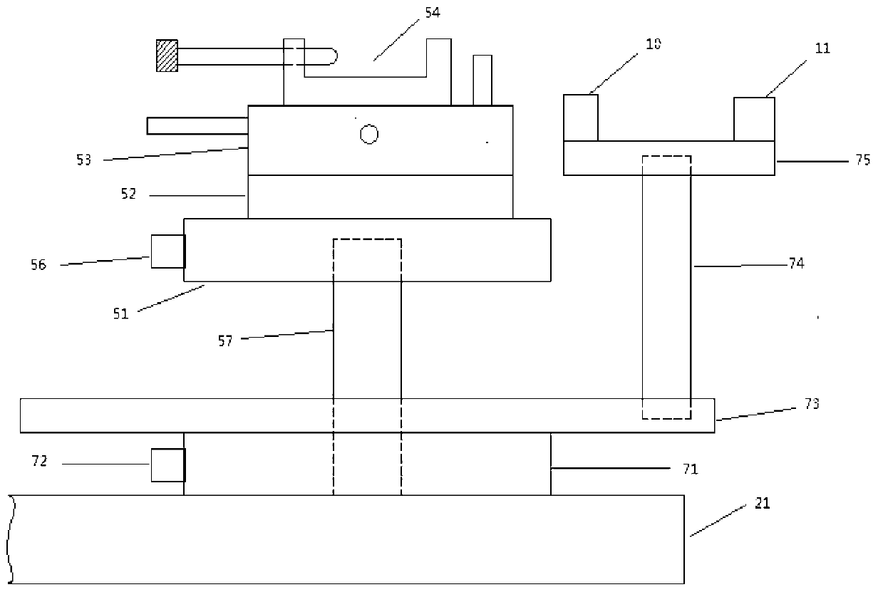
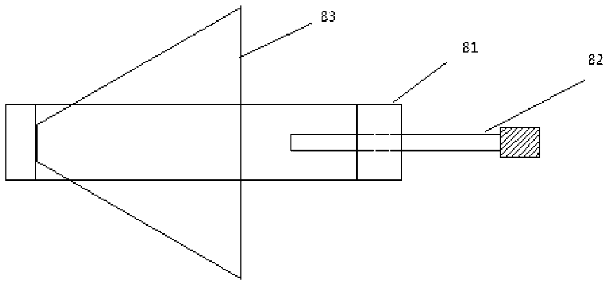
[0050] A kind of measuring device of the optical parameter of dielectric thin film that present embodiment proposes, such as figure 1 , figure 2 , image 3 , Figure 4 with Figure 5 As shown, it includes a refractive index and thickness measurement component, a transmittance and a reflectance measurement component, a sample stage component 5 for placing samples, a support component 7 , a controller 22 , a fixing base 21 and a computer terminal 23 . The refractive index and thickness measurement assembly is composed of a laser light source assembly 1, a polarizer 2, a half mirror 3, a circular aperture diaphragm 4, an autocollimation detector 6 and a measurement detector 10, a polarizer 2, a half mirror 3 and circular aperture stop 4 are sequentially arranged on the light propagation path of the laser light emitted by the laser light source assembly 1, and the laser light emitted by the laser light source assembly 1 passes through the polarizer 2 to form polarized light, a...
Embodiment 2
[0061] This embodiment proposes a method for measuring optical parameters of a dielectric thin film corresponding to the measuring device described in Embodiment 1, which includes two parts: measurement of the refractive index and thickness of the dielectric thin film, and measurement of the transmittance and reflectivity of the dielectric thin film.
[0062] Wherein, the measurement steps of the refractive index and thickness of the dielectric film are:
[0063] ①-1. Choose a piece of double-sided polished quartz glass as the substrate and clean it to prepare a polymethyl methacrylate (PMMA) solution, and coat a layer of PMMA film on the surface of the quartz glass by spin coating. After baking at 80°C for 5 hours, the sample is formed; the sample is placed on the first sample holder, and the dielectric film of the sample is closely attached to the bottom surface of the prism in the first sample holder, and then the first sample is adjusted. The micrometer screw in the sample...
PUM
| Property | Measurement | Unit |
|---|---|---|
| Thickness | aaaaa | aaaaa |
Abstract
Description
Claims
Application Information


