Transverse high-voltage power device with ultralow specific on-conduction resistance and manufacturing method of transverse high-voltage power device

A technology of specific on-resistance and lateral high voltage, applied in the field of semiconductor power devices, can solve problems such as rising on-resistance, and achieve the effect of reducing resistivity, small on-resistance, and reducing on-resistance

Active Publication Date: 2013-09-04
UNIV OF ELECTRONICS SCI & TECH OF CHINA +1
View PDF8 Cites 12 Cited by
  • Summary
  • Abstract
  • Description
  • Claims
  • Application Information

AI Technical Summary

Problems solved by technology

In the design of power LDMOS devices (Latral Double-diffused MOSFET), the breakdown voltage BV (Breakdown Voltage) and the specific on-resistance R on,sp (Specific on-resistance) There is a relationship: R on,sp ∝BV 2.3~2.6 , so when the device is applied at high voltage, the on-resistance rises sharply, which limits the application of high-voltage LDMOS devices in high-voltage power integrated circuits, especially in circuits that r...

Method used


Image

  • Transverse high-voltage power device with ultralow specific on-conduction resistance and manufacturing method of transverse high-voltage power device
  • Transverse high-voltage power device with ultralow specific on-conduction resistance and manufacturing method of transverse high-voltage power device
  • Transverse high-voltage power device with ultralow specific on-conduction resistance and manufacturing method of transverse high-voltage power device

Examples


Embodiment Construction

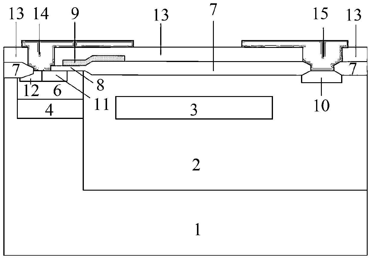
[0035] The present invention provides a horizontal high-voltage power device realized by ion implantation process, which has low process difficulty and strong operability. By selecting different types of substrates and impurities, n-channel and p-channel horizontal high-voltage power devices can be manufactured .

[0036] figure 1 The structure diagram of a traditional lateral high voltage DMOS device with a field drop layer structure is given, including a first conductivity type semiconductor substrate 1, a second conductivity type semiconductor drift region 2, a first conductivity type semiconductor drop field layer 3, and a first conductivity type Semiconductor body region 6, field oxide layer 7, gate oxide layer 8, polysilicon gate electrode 9, second conductivity type semiconductor drain region 10, second conductivity type semiconductor source region 11, body contact region 12, pre-metal dielectric 13, source electrode Metal 14 and drain metal 15.

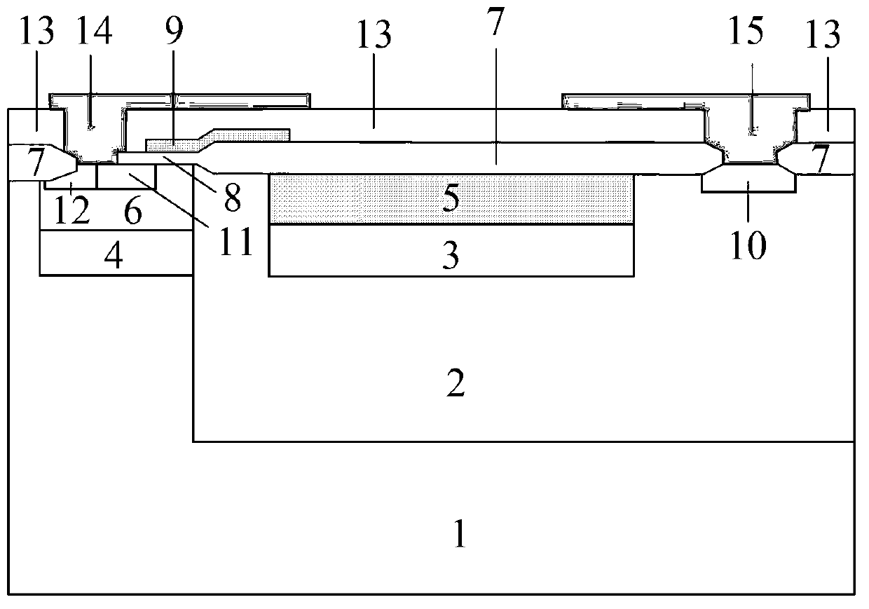
[0037] figure 2 It is a ...


PUM

PropertyMeasurementUnit
Thicknessaaaaaaaaaa

Abstract

The invention relates to a transverse high-voltage power device with ultralow specific on-resistance and a manufacturing method of the transverse high-voltage power device and belongs to the technical field of a power semiconductor device. Through photoetching and ion implantation processes, a second conducting type semiconductor heavy doping layer (5) formed at the surface of a second conducting type semiconductor drift region (2) provides a low-resistance surface conduction passage for the device during the on state and provides two conduction passages for the device together with the second conducting type semiconductor drift region (2) arranged under a reduced field layer (3). Because the ion implantation is adopted, the low-resistance surface conduction passages are added, the surface electric resistivity of the device is reduced, and the on resistance of the device is greatly reduced. Compared with an ordinary high-voltage device with the reduced field layer, the transverse high-voltage power device provided by the invention has smaller on resistance under the condition of the same chip area (or the transverse high-voltage power device has smaller chip area under the condition of the same conduction capability). The transverse high-voltage power device can be applied to various products such as consumer electronics and display driving products.

Description

Technical field [0001] The invention belongs to the technical field of semiconductor power devices, and relates to a lateral high-voltage power device with ultra-low specific on-resistance and a manufacturing method thereof. Background technique [0002] Lateral high-voltage power devices are an essential part of the development of high-voltage power integrated circuits. High-voltage power devices require high breakdown voltage, low on-resistance and low switching losses. The lateral high voltage power device achieves high breakdown voltage, and the drift region used to bear the withstand voltage is required to have a long size and low doping concentration. However, in order to meet the low on-resistance of the device, the drift region as a current channel is required to have High doping concentration. In the design of power LDMOS devices (Latral Double-diffused MOSFET), the breakdown voltage BV (Breakdown Voltage) and the specific on-resistance R on,sp (Specific on-resistance) ...

Claims


Application Information

Patent Timeline
IPC IPC(8): H01L29/78H01L29/10H01L21/336
Inventor 乔明李燕妃周锌蔡林希许琬吴文杰张波
Owner UNIV OF ELECTRONICS SCI & TECH OF CHINA
Why Eureka
Try Eureka