Method for preparing crystalline silicon heterojunction/microcrystalline silicon thin film laminated photovoltaic cell

A microcrystalline silicon thin film and photovoltaic cell technology, which is applied in the field of solar cells, can solve the problems of consuming chemicals, limiting the increase of open circuit voltage, and resource constraints of indium elements.

Inactive Publication Date: 2013-09-04
ZHEJIANG ASTRONERGY
View PDF8 Cites 3 Cited by
  • Summary
  • Abstract
  • Description
  • Claims
  • Application Information

AI Technical Summary

Problems solved by technology

This process is very difficult to control and consumes a lot of valuable chemicals, while the corrosion reaction consumes valuable silicon wafer material
Due to the very rough texture of the surface, it is difficult to completely cover the rough surface with the extremely thin silicon and p-type amorphous silicon film (total thickness 10nm-30nm) during the formation of the heterojunction, which severely limits the open circuit voltage. promote
On the other hand, traditional heterojunction cells use sputtered ITO as the conductive oxide (TCO) material. ITO materials are very expensive, and the indium element is severely limited by resources, which causes serious resource bottlenecks for large-scale utilization of solar energy.
Although the efficiency of heterojunction cells is high, the complex structure and process steps, coupled with expensive materials, seriously hinder the promotion of heterojunction cells
[0009] A Chinese patent application (Application No.: 201210041796.6) discloses a stacked battery structure, the thin-film battery in the stacked battery is an amorphous silicon battery, which has a large light-induced attenuation problem
In addition, in this patent, neither the heterojunction cell nor the amorphous silicon thin-film cell has a light-trapping structure, and the 80nm-100nm conductive film mentioned in the publication cannot form a light-trapping effect, which will cause the cell to be used in practice. Difficulty in application
[0010] Chinese patent application (Application No. 201210292308.9) discloses a stacked battery using p-type silicon wafer heterojunction and amorphous silicon thin film battery. This patent application also does not solve the problem of light-induced attenuation of amorphous silicon thin film battery
Since the heterojunction cell part of the laminated battery uses p-type amorphous silicon material, the open circuit voltage of the high-low junction formed with the p-type silicon wafer will be very low, and the battery will have great difficulties in practical application; in addition, the The patent uses 60nm~100nm sputtering TCO layer, such TCO layer has no light trapping effect at all
[0011] Chinese patent application (Application No. 201210292258.4) discloses a stacked battery, but the battery of this structure is not connected in series, and the voltage cannot be superimposed. It is actually a double-sided heterojunction battery.
The patent application uses ZnO on the silicon wafer to increase reflection, but this structure completely loses the meaning of heterojunction, and it is actually impossible to form a heterojunction across the ZnO layer
That is, the patent application is actually a heterojunction-heterojunction stacked structure, which will cause the battery to fail to work

Method used


Image

  • Method for preparing crystalline silicon heterojunction/microcrystalline silicon thin film laminated photovoltaic cell
  • Method for preparing crystalline silicon heterojunction/microcrystalline silicon thin film laminated photovoltaic cell
  • Method for preparing crystalline silicon heterojunction/microcrystalline silicon thin film laminated photovoltaic cell

Examples


Embodiment Construction

[0039] The following disclosure provides many different embodiments or examples for implementing different structures of the present invention. To simplify the disclosure of the present invention, components and arrangements of specific examples are described below. Furthermore, the present invention may repeat reference numerals and / or letters in different instances. This repetition is for the purpose of simplicity and clarity and does not in itself indicate a relationship between the various embodiments and / or arrangements discussed. It should be noted that components illustrated in the figures are not necessarily drawn to scale. Descriptions of well-known components and processing techniques and processes are omitted herein to avoid unnecessarily limiting the present invention.

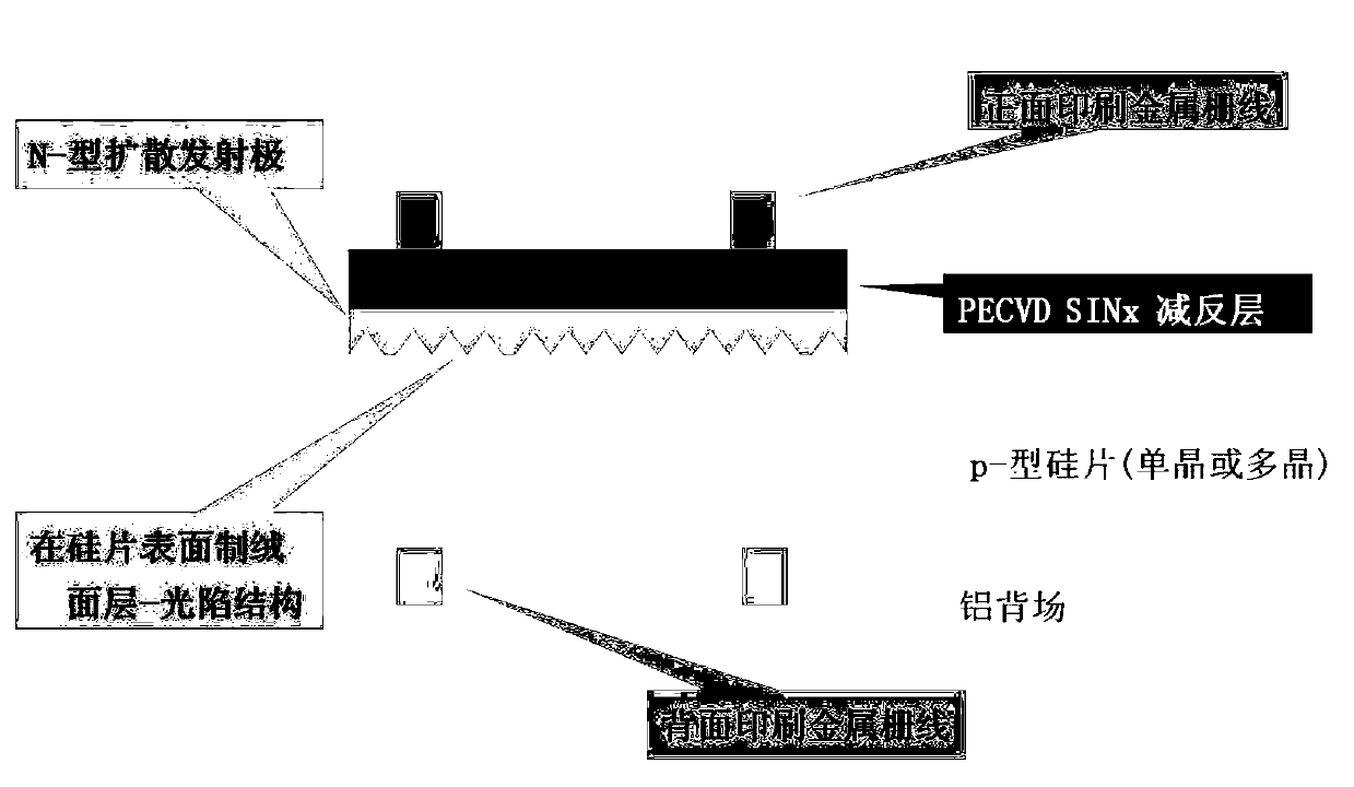
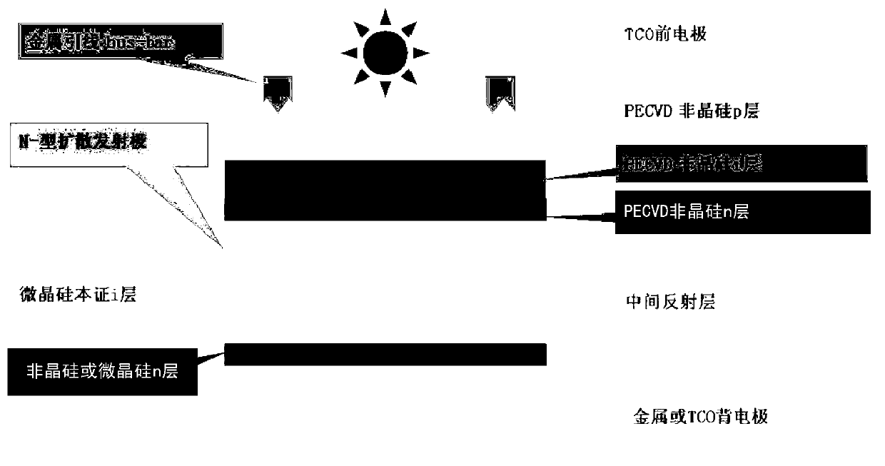
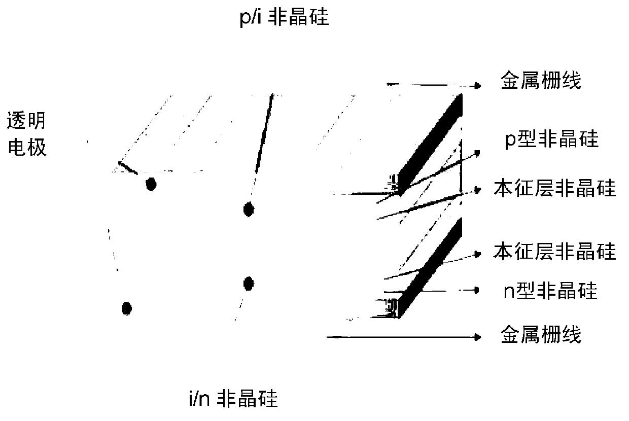
[0040] refer to Figure 4 and Figure 8 , Figure 8 It is a schematic flow chart of a method for preparing a crystalline silicon heterojunction / microcrystalline silicon thin film stack photovo...


PUM

PropertyMeasurementUnit
thicknessaaaaaaaaaa
thicknessaaaaaaaaaa
thicknessaaaaaaaaaa

Abstract

The invention discloses a method for preparing a crystalline silicon heterojunction / microcrystalline silicon thin film laminated photovoltaic cell. The preparation method includes the following steps that a first amorphous silicon intrinsic i layer and an amorphous silicon p layer are sequentially formed on a n-type silicon slice; a second amorphous silicon intrinsic i layer and an amorphous silicon n layer are sequentially formed at the back of the n-type silicon slice; a first boron-doped zinc oxide thin film is formed on the amorphous silicon p layer; an n-i-p structure is formed on the first boron-doped zinc oxide thin film; a second boron-doped zinc oxide thin film is formed on the n-i-p structure, and a third boron-doped zinc oxide thin film is formed on the amorphous silicon n layer; back electrodes are formed at the back of the n-type silicon slice, and front electrodes are formed at the front of the n-type silicon slice. By the adoption of the preparation method, open-circuit voltage of a solar cell can be greatly improved, and photoelectric conversion efficiency of the solar cell is effectively improved.

Description

technical field [0001] The invention relates to the technical field of solar cells, in particular to a method for preparing a crystalline silicon heterojunction / microcrystalline silicon thin film stacked photovoltaic cell. Background technique [0002] In recent years, amazing progress has been made in the application of photovoltaic cells, and the price of components has dropped sharply, opening the way for large-scale utilization of solar power generation. Crystalline silicon solar cells have the advantages of high conversion efficiency and mature production technology, and have always occupied the vast majority of the world's total output of solar cells. Although the technical level of crystalline silicon solar cells has been steadily improving, the high-temperature diffusion junction process and lack of a good surface passivation mechanism in the production process of traditional crystalline silicon solar cells limit the further improvement of the photoelectric conversio...

Claims


Application Information

Patent Timeline
Patent Type & Authority Applications(China)
IPC IPC(8): H01L31/20
CPCY02P70/50
Inventor 牛新伟刘石勇戎俊梅丁澜韩玮智金建波陆川仇展炜
Owner ZHEJIANG ASTRONERGY
Why Eureka
Try Eureka