Method for forming channel of thin film transistor and compensating circuit

A thin-film transistor and compensation circuit technology, applied in transistors, circuits, electrical components, etc., can solve the problems of decreased electron mobility, uneven electrical properties of TFT, low electron mobility, etc., achieve uniform electrical properties, and improve electron mobility. Effect

Inactive Publication Date: 2013-09-25
TCL CHINA STAR OPTOELECTRONICS TECH CO LTD
View PDF6 Cites 5 Cited by
  • Summary
  • Abstract
  • Description
  • Claims
  • Application Information

AI Technical Summary

Problems solved by technology

[0006] When the channel length of the TFT is parallel to the grain boundary of the polysilicon film, the electron mobility is higher, for example, 300cm 2 / V-s; but if the channel length of the TFT is perpendicular to the grain boundary of the polysilicon film, the electron mobility of the TFT will be greatly reduced to 100cm 2 / V-s, so in the SLS lateral crystallization technology in the prior art, the electron mobility of the TFT channel is low, and the electrical inhomogeneity of the TFT

Method used


Image

  • Method for forming channel of thin film transistor and compensating circuit
  • Method for forming channel of thin film transistor and compensating circuit
  • Method for forming channel of thin film transistor and compensating circuit

Examples


Embodiment Construction

[0023] The following descriptions of the various embodiments refer to the accompanying drawings to illustrate specific embodiments in which the present invention can be practiced. The directional terms mentioned in the present invention, such as "up", "down", "front", "back", "left", "right", "inside", "outside", "side", etc., are for reference only The orientation of the attached schema. Therefore, the directional terms used are used to illustrate and understand the present invention, but not to limit the present invention. In the figures, structurally similar units are denoted by the same reference numerals.

[0024] see Figures 1A-1M , Figures 1A-1M It is a schematic diagram of the process of the channel formation method of the thin film transistor array substrate in the embodiment of the present invention.

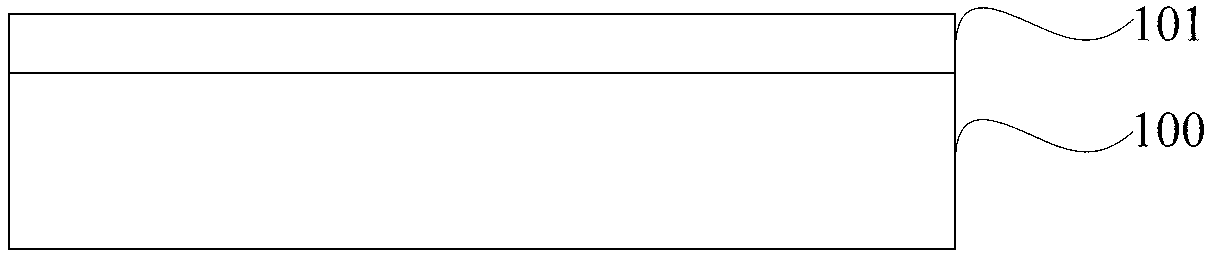
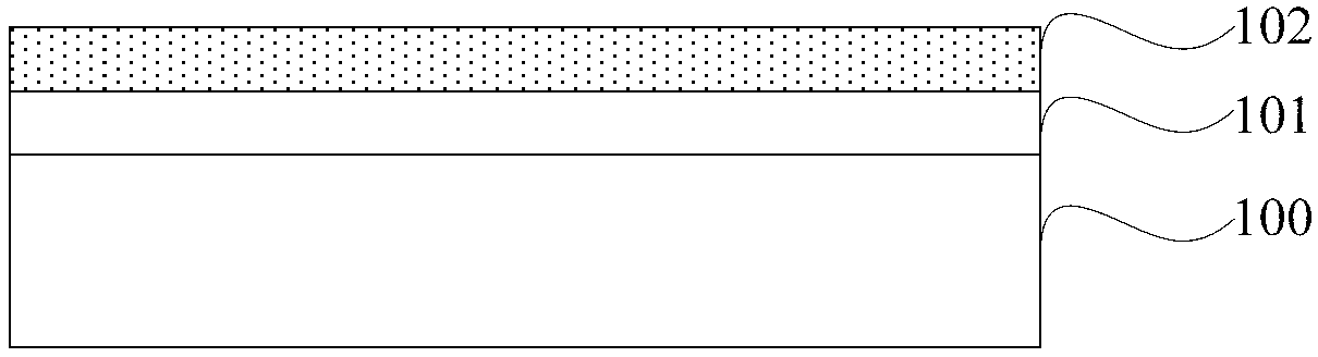
[0025] exist Figure 1A In the present invention, a substrate 100 is provided, and a buffer layer 101 (Buffer) is formed on the substrate 100 .
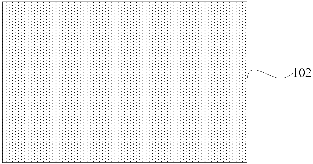
[0026] Wherein ...


PUM


Abstract

The invention discloses a method for forming a channel of a thin film transistor and a compensating circuit. The method for forming the channel of the thin film transistor comprises the steps of (1) forming amorphous silicon layers on a substrate; (2) carrying out etching processing on the amorphous silicon layer to form an amorphous silicon graph which comprises a plurality of amorphous silicon layers, wherein each amorphous silicon layer of the amorphous silicon graph is of a bent structure; (3) forming two disconnected spaces in each amorphous silicon layer of the amorphous silicon layer, wherein every two disconnected spaces are formed at adjacent bent positions of each amorphous silicon layer respectively; (4) carrying out laser irradiation processing on the amorphous silicon graph which has the disconnected spaces so as to enable crystal grains, on the two sides of each disconnected space, of each amorphous silicon layer to grow towards a corresponding disconnected space under the action of the temperature difference, and carrying out crystallization to form the channel of the thin film transistor in each disconnected space. The method for forming the channel of the thin film transistor and the compensating circuit can improve the electron mobility of the formed channel, and the electrical property is more even.

Description

【Technical field】 [0001] The invention relates to the technical field of liquid crystal display, in particular to a method for forming a channel of a thin film transistor and a compensation circuit. 【Background technique】 [0002] Thin Film Transistor (Thin Film Transistor, TFT) has been widely used in the driving of active liquid crystal displays, and the silicon thin film material used according to the thin film transistor usually has two types: amorphous silicon (amorphous-silicon) and polysilicon (poly-silicon). . [0003] In the manufacture of liquid crystal displays, polycrystalline silicon materials have many characteristics superior to amorphous silicon materials. Polysilicon has larger grains, allowing electrons to easily move freely in polysilicon, so the electron mobility (mobility) of polysilicon is higher than that of amorphous silicon. Thin film transistors made of polysilicon have a faster response time than amorphous silicon thin film transistors. In a liq...

Claims


Application Information

Patent Timeline
Patent Type & Authority Applications(China)
IPC IPC(8): H01L21/336H01L29/786H01L29/10G09G3/34
CPCH01L21/268H01L27/1281H01L27/1285H01L29/66757H01L29/78675
Inventor 许宗义
Owner TCL CHINA STAR OPTOELECTRONICS TECH CO LTD
Why Eureka
Try Eureka