

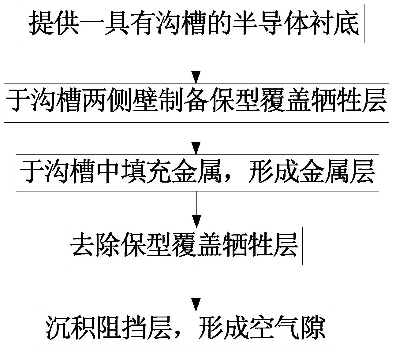
Air gap forming method
An air gap and trench technology, applied in electrical components, semiconductor/solid-state device manufacturing, circuits, etc., can solve the problems of increasing device manufacturing costs, losing more raw materials, increasing production costs, etc., achieving less consumables, improving production efficiency, Improve the effect of RC delay
- Summary
- Abstract
- Description
- Claims
- Application Information
AI Technical Summary
Problems solved by technology
Method used
Image

Examples
Embodiment 1
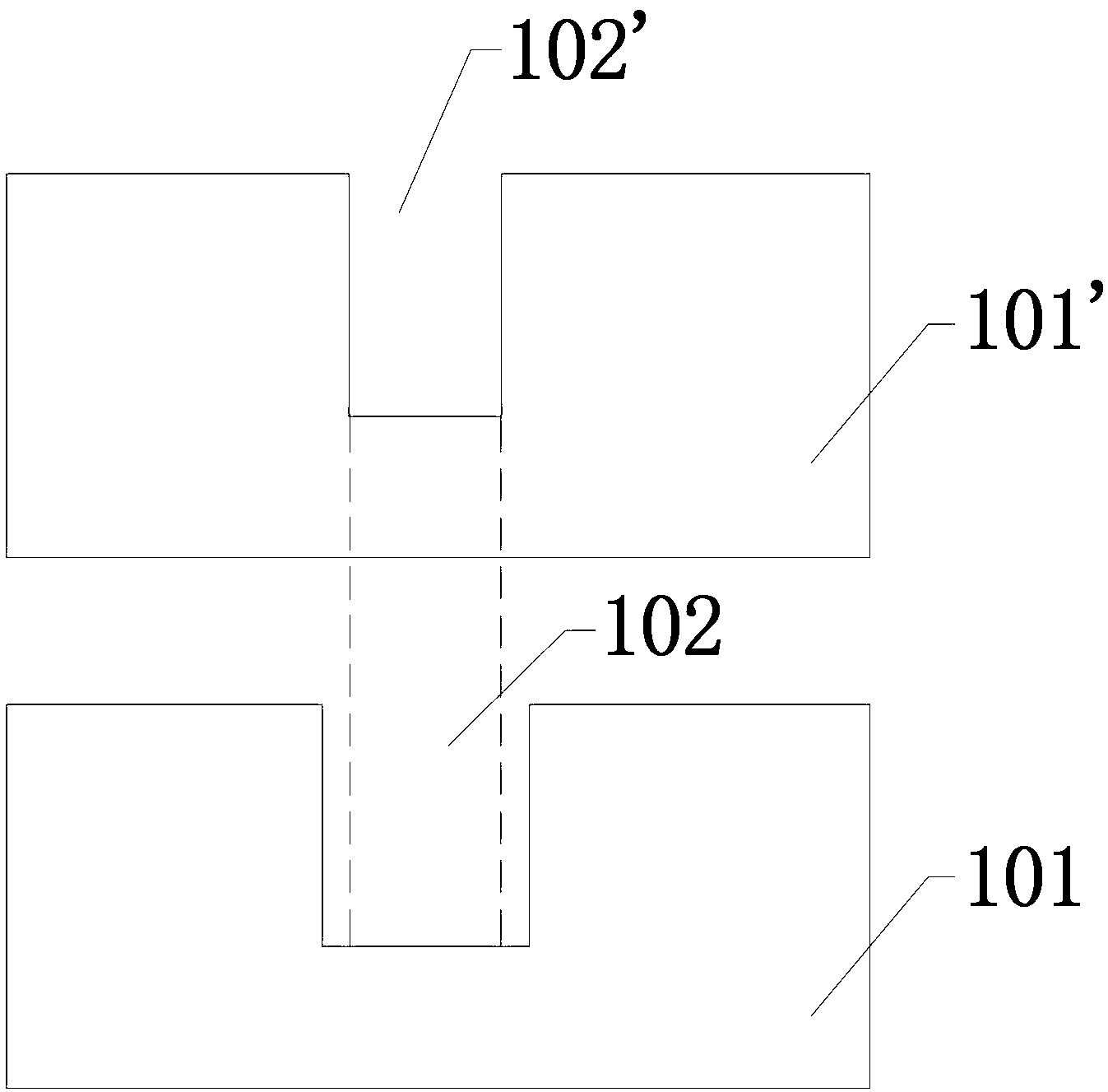
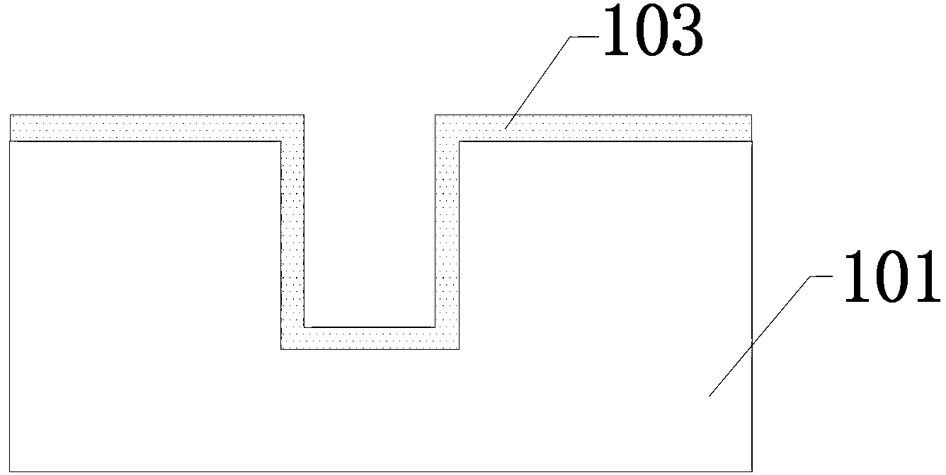
[0061] figure 2 It is a schematic diagram of the comparison between the critical dimensions of the trench design in the traditional process and the key dimensions of the trench design provided in Example 1 of the present invention; as shown in the figure, in the traditional process, the critical dimension of the trench design and the process requirements The critical dimensions are the same, and after subsequent photolithography, etching and wet processing processes, a trench 102' is formed on the semiconductor substrate 101', wherein the wet processing uses ST250 (organic chemicals, here is the American AIMI The company's commercially available organic chemicals (AIMI ST250) liquid medicine and DHF (Dilute Hydrogen Fluoride, dilute hydrofluoric acid solution, non-polar chemical) liquid medicine are used to prevent the existence of residual particles in the groove; in the process of the present invention, the design The critical dimension of the trench is larger than the crit...
PUM
 Abstract
Description
Claims
Application Information