High heat conduction substrate and manufacturing method thereof

A high thermal conductivity, substrate technology, applied in printed circuit manufacturing, printed circuit parts, electrical components, etc., can solve the problems of easy diffusion, insulation decline, low thermal expansion coefficient, etc., and achieve the solution of buffer layer metal diffusion and stable performance Effect

Active Publication Date: 2013-09-25
SUN YAT SEN UNIV
View PDF6 Cites 16 Cited by
  • Summary
  • Abstract
  • Description
  • Claims
  • Application Information

AI Technical Summary

Problems solved by technology

The method mentioned in Patent No. 200810149489.3 is to use copper as a buffer layer, but copper is easy to diffuse into the porous insulating layer, which reduces the insulation
In this regard, the inventor's solution is to add a barrier layer composed of tungsten, titanium, tantalum or their alloys between the buffer layer and the insulating layer. However, the thermal conductivity of titanium is only 21.9 W·m -1·K-1, only one tenth of aluminum (220W·m-1·K-1) First, it seriously affects the heat dissipation effect; and the thermal expansion coefficient of tantalum and tungsten is even lower than that of alumina (tantalum is 6×10⁻⁶ / ℃, tungsten is only 4.5×10⁻⁶ / ℃), contrary to the purpose of adding a buffer layer

Method used


Image

  • High heat conduction substrate and manufacturing method thereof

Examples


preparation example Construction

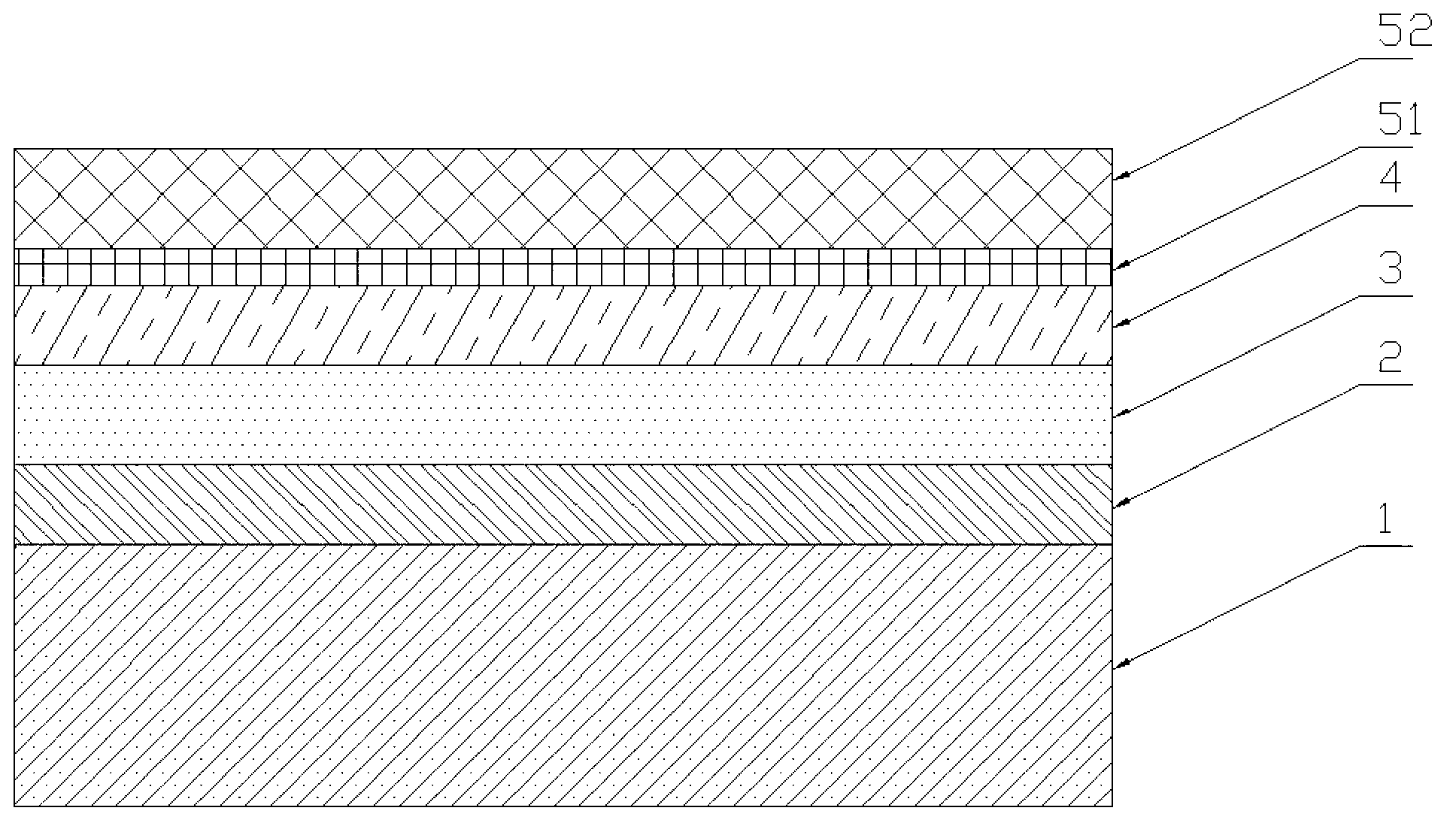
[0028] A method for preparing a high thermal conductivity substrate, characterized in that: comprising the following steps:

[0029] 1) A layer of aluminum is formed on one side of the alloy buffer layer by physical vapor deposition or hot-dip plating to form a connection layer between the aluminum substrate and the buffer layer, and then the alloy buffer layer is connected to the aluminum substrate by diffusion welding;

[0030] 2) Cover a layer of aluminum on the other side of the buffer layer by physical vapor deposition or hot-dip plating;

[0031] 3) Use anodic oxidation or micro-arc oxidation to convert the aluminum layer in the previous step into an aluminum oxide insulating layer;

[0032] 4) A primary conductive layer is formed on the surface of the insulating layer by physical vapor deposition; a secondary conductive layer is formed on the surface of the primary conductive layer by electrochemical deposition.

[0033] The anodic oxidation solution used in the anodic...

Embodiment 1

[0040] A method for preparing a high thermal conductivity substrate, comprising the steps of:

[0041] 1) A layer of 10 μm metal aluminum is formed on one side of the 50 μm molybdenum-copper alloy buffer layer by evaporation, which is used as the connection layer between the aluminum substrate and the buffer layer;

[0042] 2) The buffer layer and the aluminum substrate are connected by the connection layer by means of diffusion welding;

[0043] 3) Cover the other side of the molybdenum-copper alloy buffer layer with an aluminum layer by evaporation plating (the thickness of the aluminum layer is such that after anodic oxidation becomes an insulating layer, the thickness of the insulating layer is 10 μm);

[0044] 4) Through anodic oxidation, the aluminum layer is converted into an aluminum oxide insulating layer;

[0045] 5) The conductive layer is processed in this way: first magnetron sputtering metallic silver 300 ?

[0046] The coefficient of thermal expansion of the all...

Embodiment 2

[0050] A method for preparing a high thermal conductivity substrate, comprising the steps of:

[0051] 1) Form a layer of 50 μm metal aluminum on one side of the 200 μm titanium-copper alloy buffer layer by evaporation, and use it as the connection layer between the aluminum substrate and the buffer layer;

[0052] 2) The buffer layer and the aluminum substrate are connected by the connection layer by means of diffusion welding;

[0053] 3) Cover the other side of the titanium-copper alloy buffer layer with an aluminum layer by hot-dip plating (the thickness of the aluminum layer is such that after micro-arc oxidation becomes an insulating layer, the thickness of the insulating layer is 100 μm);

[0054] 4) Through micro-arc oxidation, the aluminum layer is converted into an aluminum oxide insulating layer;

[0055] 5) The conductive layer is processed in this way: first magnetron sputtering metal silver 850? on the insulating layer to realize its conductivity, and then elect...


PUM

PropertyMeasurementUnit
Thicknessaaaaaaaaaa
Thicknessaaaaaaaaaa
Thermal expansion coefficientaaaaaaaaaa

Abstract

The invention discloses a high heat conduction substrate which comprises an aluminum base material. A connecting layer, an alloy buffering layer, an insulating layer and a conducting layer are sequentially arranged on the surface of the aluminum base material, wherein the conducting layer is formed by a first-stage conducting layer body and a second-stage conducting layer body covering the surface of the first-stage conducting layer body in a combined mode. A manufacturing method of the high heat conduction substrate includes the steps of (1) forming a layer of aluminum on one face of the alloy buffering layer to form the connecting layer for connecting the aluminum base material with the alloy buffering layer, (2) covering a layer of aluminum on the other face of the alloy buffering layer through physical vapor deposition or hot dipping, (3) converting the aluminum layer in the last step into an aluminum oxide insulating layer through the anodic oxidation method or micro-arc oxidation, (4) forming the first-stage conducting layer body on the surface of the insulating layer through the physical vapor deposition, and (5) forming the second-stage conducting layer body on the surface of the first-stage conducting layer body through the electrochemical deposition method. The high heat conduction substrate is stable in performance at the high temperature, cannot crack, and meanwhile solves the problem of metal diffusion of the buffering layer effectively.

Description

technical field [0001] The invention relates to a high thermal conductivity substrate and a preparation method thereof. Background technique [0002] In recent years, the electronic industry has developed vigorously, various high-power electronic components emerge in an endless stream, and the density of components on circuit boards is also increasing. This makes the heat generated greatly increase while the energy consumption increases. If the heat cannot be transferred in time, it will affect the performance of the components. The traditional insulating substrate made of epoxy resin has a large thermal resistance, which is far from meeting the needs of high-power heat dissipation; the substrate made of ceramic materials, although its thermal conductivity is far greater than that of epoxy resin, the gap between the substrate and the radiator The connection between them requires the use of thermally conductive adhesive, and the thermal resistance of the thermally conductiv...

Claims


Application Information

Patent Timeline
IPC IPC(8): H05K1/02H05K3/00
Inventor 崔国峰陆航宇
Owner SUN YAT SEN UNIV
Why Eureka
Try Eureka