Method for low-temperature deposition of InN film on glass substrate
A glass substrate, low temperature technology, applied in gaseous chemical plating, metal material coating process, coating and other directions, can solve the problems of difficult to reduce device cost, high price of sapphire substrate, hinder the development of InN material devices, etc. The effect of low cost and good electrical performance
- Summary
- Abstract
- Description
- Claims
- Application Information
AI Technical Summary
Problems solved by technology
Method used
Image
Examples
Embodiment 1
[0036] After the Corning glass substrate was ultrasonically cleaned with acetone, ethanol and deionized water in sequence, it was blown dry with nitrogen and sent to the reaction chamber.
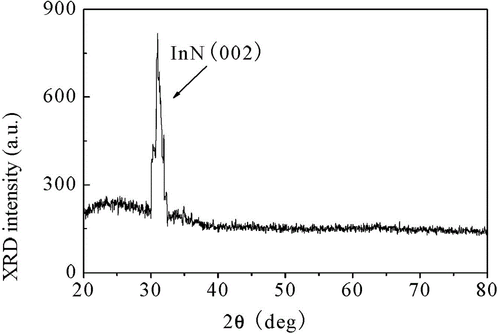
[0037] Evacuate the reaction chamber to 8.0 × 10 -4 Pa, when the substrate is not heated to a room temperature of 20°C, trimethylindium and nitrogen carried by hydrogen are introduced into the reaction chamber, and the flow ratio of trimethylindium and nitrogen reaction source is controlled at 2:100, and the flow rate is determined by the mass flowmeter Control, the flow parameters are 2sccm and 100sccm respectively; the total pressure of the control gas is 0.8Pa; the electron cyclotron resonance power is 650W, the reaction is 30min, and the InN photoelectric thin film on the Corning glass substrate is obtained.
[0038] After the experiment, the Hall test equipment was used to test and analyze the mobility and carrier concentration of the film. The results are shown in Table 1. It can be...
Embodiment 2
[0042] After the Corning glass substrate was ultrasonically cleaned with acetone, ethanol and deionized water in sequence, it was blown dry with nitrogen and sent to the reaction chamber.
[0043] Evacuate the reaction chamber to 8.0 × 10 -4 Pa, the substrate is heated to 100°C, trimethylindium and nitrogen carried by hydrogen are introduced into the reaction chamber, and the flow ratio of trimethylindium and nitrogen reaction source is controlled at 2:150, which is controlled by the flow rate of the mass flow meter. The parameters are 2sccm and 150sccm respectively; the total pressure of the control gas is 2.0Pa; the electron cyclotron resonance power is 650W, and the reaction is 70min to obtain the InN photoelectric thin film on the Corning glass substrate.
[0044] After the experiment, the Hall test equipment was used to test and analyze the mobility and carrier concentration of the film. The results are shown in Table 2. It can be seen from Table 2 that the InN thin fil...
Embodiment 3
[0048] After the Corning glass substrate was ultrasonically cleaned with acetone, ethanol and deionized water in sequence, it was blown dry with nitrogen and sent to the reaction chamber.
[0049] Evacuate the reaction chamber to 8.0 × 10 -4 Pa, the substrate is heated to 200°C, trimethylindium and nitrogen carried by hydrogen gas are introduced into the reaction chamber, and the flow ratio of trimethylindium and nitrogen reaction source is controlled at 3:200, which is controlled by the flow rate of the mass flow meter. The parameters are 3 sccm and 200 sccm respectively; the total pressure of the control gas is 1.5Pa; the electron cyclotron resonance power is 650W, and the reaction is 120min, and the InN photoelectric thin film on the Corning glass substrate is obtained.
[0050] After the experiment, the Hall test equipment was used to test and analyze the mobility and carrier concentration of the film. The results are shown in Table 3. It can be seen from Table 3 that th...
PUM
| Property | Measurement | Unit |
|---|---|---|
| thickness | aaaaa | aaaaa |
| thickness | aaaaa | aaaaa |
Abstract
Description
Claims
Application Information


