
Growing method for duplex multi-quantum well luminescent layer structure and LED epitaxial structure

A technology of multiple quantum wells and growth methods, applied in the field of LED epitaxy design, can solve problems such as insufficient brightness of LED chips, achieve the effects of improving the low hole concentration, improving efficiency, and increasing recombination probability

Active Publication Date: 2013-10-09
XIANGNENG HUALEI OPTOELECTRONICS
View PDF2 Cites 10 Cited by
  • Summary
  • Abstract
  • Description
  • Claims
  • Application Information

AI Technical Summary

Problems solved by technology

[0006] The purpose of the present invention is to provide a growth method of a composite multi-quantum well light-emitting layer structure and a corresponding LED epitaxial structure, so as to solve the technical problem of insufficient brightness of the current LED chip

Method used


Image

  • Growing method for duplex multi-quantum well luminescent layer structure and LED epitaxial structure
  • Growing method for duplex multi-quantum well luminescent layer structure and LED epitaxial structure
  • Growing method for duplex multi-quantum well luminescent layer structure and LED epitaxial structure

Examples


Embodiment 1

[0062] The invention uses AixtronCruisIIMOCVD to grow high-brightness GaN-based LED epitaxial wafers. Using high-purity H 2 or high purity N 2 or high purity H 2 and high purity N 2 The mixed gas is used as carrier gas, high-purity NH3 is used as N source, trimethylgallium (TMGa) and triethylgallium (TEGa) are used as gallium source, trimethylindium (TMIn) is used as indium source, silane (SiH 4 ) as N-type dopant, trimethylaluminum (TMAl) as aluminum source, dimagnesocene (CP 2 Mg) is used as a P-type dopant, the substrate is (0001) sapphire, and the reaction chamber pressure is between 150mbar and 600mbar.

[0063] 1. Under the hydrogen atmosphere of 1000-1100℃, the pressure of the reaction chamber is controlled at 150-200mbar, and the sapphire substrate is treated at high temperature for 4-5 minutes;

[0064] 2. Lower the temperature to 540-570°C, control the pressure of the reaction chamber at 450-600mbar, and grow a low-temperature buffer layer GaN with a thickness o...

Embodiment 2

[0091] For the implementation steps, refer to Example 1 to obtain sample 4.

[0092] The comparison of growth parameters between Comparative Example 2 and Example 2 can be seen in Table 2 below.

[0093]Table 2 contrasts the growth parameters of Example two and Example two

[0094]

[0095] Then, take sample 3 and sample 4 to take the same treatment method as sample 1 and sample 2 and then test the photoelectric performance of sample 3 and sample 4, the parameters obtained can be found in Figure 6 . Figure 6 The vertical axis of is the brightness (Lm), and the horizontal axis is the distribution number of chip particles. The value corresponding to sample 4 is the upper thicker line, and the value corresponding to sample 3 is the lower thinner line. From Figure 6 According to the data, the brightness of sample 4 is 8-9% higher than that of sample 3. The growth method provided by this patent improves the light efficiency of large-size chips.

[0096] see figure 2 ...


PUM


Abstract

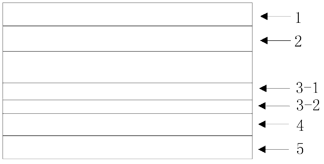
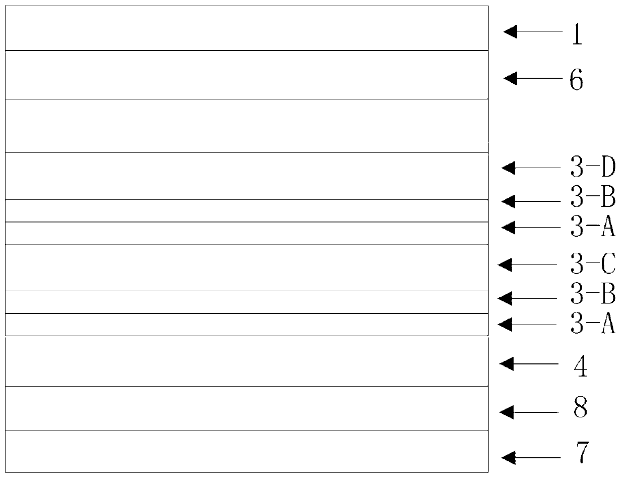
The invention provides a growing method for a duplex multi-quantum well luminescent layer structure and an LED epitaxial structure. A well luminescent layer of the epitaxial structure comprises six to eight unit layers, wherein each unit layer comprises a first well layer, a second well layer, a first epitaxial layer, a first well layer, a second well layer and a second epitaxial layer from top to bottom in sequence. According to the growing method for a duplex multiple-quantum well luminescent layer structure and the LED epitaxial structure, a duplex multiple-quantum well is adopted, the situation that separation of wave functions is caused by the stress of well layers and epitaxial layers in a traditional multi-quantum well is improved, and the situation that the hole concentration of the well layers is too low due to the epitaxial width in the traditional multi-quantum well is improved. Efficiency obtaining of the quantum well inside an LED chip is improved, the brightness of medium and small size LED chips is improved in macro view, and the lighting effects of large size LED chips are improved.

Description

technical field [0001] The invention relates to the technical field of LED epitaxial design, in particular to a method for growing a compound multi-quantum well light-emitting layer structure and a corresponding LED epitaxial structure. Background technique [0002] In the LED market, large-size and high-power 30mil*30mi chips are mostly used for street lighting, and small and medium-sized 12mil*28mil chips are mostly used for backlighting. The quality of the products is related to the brightness of the chip. Therefore, the brightness of chips of various sizes has become the focus of packaging customers. [0003] At present, there are many epitaxial growth methods to improve the light efficiency of large size and the brightness of small and medium size. Most of the structural innovations lie in the P-type layer, such as: [0004] (1) The P layer adds PAlGaN / PInGaN, PAlGaN / PGaN, PAlGaN / GaN and other superlattice structures to improve the current expansion ability and achieve...

Claims


Application Information

Patent Timeline
Patent Type & Authority Applications(China)
IPC IPC(8): H01L33/00H01L33/06
Inventor 张宇
Owner XIANGNENG HUALEI OPTOELECTRONICS
Learn More