

A patterned ceramic layer printed circuit substrate for optical and electronic devices
A technology of printed circuit boards and electronic devices, which is applied in the direction of printed circuits connected with non-printed electrical components, printed circuit components, etc., can solve the problems of electrical conduction short circuit, heat transfer difficulties, etc., and achieve good electrical isolation and thermal stability. Effects of isolation, heat dissipation resolution, effective heat conduction and transfer
- Summary
- Abstract
- Description
- Claims
- Application Information
AI Technical Summary
Problems solved by technology
Method used
Image

Examples
Embodiment 1
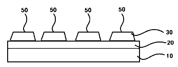
[0024] as attached figure 1 As shown, the patterned ceramic layer printed circuit substrate for optical and electronic devices described in this embodiment includes an aluminum or aluminum alloy substrate 10, on which Al 2 o 3 A pressure-resistant ceramic layer 20, and on the pressure-resistant ceramic layer 20, a patterned AlN high thermal conductivity ceramic layer 30 is deposited through a baffle using a magnetron sputtering deposition method, and a plurality of thermally conductive isolation bases 50 are formed; and in the A metal circuit layer (not shown in the figure) is formed on the high thermal conductivity ceramic layer of the thermal conductivity isolation base. The Al 2 o 3 The pressure-resistant ceramic layer is prepared by the following process, and the reaction system is AlCl 3 -H 2 O-O 2 -H 2 , the reaction temperature is 420-500°C, the working pressure is 1200Pa, where AlCl 3 The flow rate is 50 ml / min, H 2 The flow rate of O is 10-20 ml / min, O 2 The...
Embodiment 2
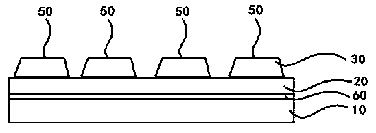
[0026] as attached figure 2 As shown, the patterned ceramic layer printed circuit substrate for optical and electronic devices described in this embodiment includes an aluminum or aluminum alloy substrate 10, on which Al 2 o 3 A pressure-resistant ceramic layer 20, and on the pressure-resistant ceramic layer 20, a patterned AlN high thermal conductivity ceramic layer 30 is deposited through a baffle using a magnetron sputtering deposition method, and a plurality of thermally conductive isolation bases 50 are formed; and in the There is an aluminum transition layer 60 between the substrate 10 and the pressure-resistant ceramic layer 20; and a metal circuit layer (not shown in the figure) is formed on the thermally conductive isolation base with high thermally conductive ceramic layer. The aluminum transition layer is prepared by the following process: the degree of vacuuming is 5.0×10 -4 Pa, feed the Ar with a purity of 99.99% into the vacuum coating chamber, flow 20sccm, an...
Embodiment 3
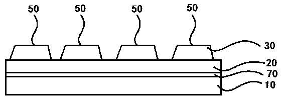
[0028] as attached image 3 As shown, the patterned ceramic layer printed circuit substrate for optical and electronic devices described in this embodiment includes an aluminum or aluminum alloy substrate 10, on which Al 2 o 3 A pressure-resistant ceramic layer 20, and on the pressure-resistant ceramic layer 20, a patterned AlN high thermal conductivity ceramic layer 30 is deposited through a baffle using a magnetron sputtering deposition method, and a plurality of thermally conductive isolation bases 50 are formed; and in the There is an active brazing layer 70 between the substrate 10 and the pressure-resistant ceramic layer 20; and a metal circuit layer (not shown in the figure) is formed on the high thermal conductivity ceramic layer of the thermally conductive isolation base. The solder of the active brazing layer is prepared by the above-mentioned water mist method, and the solder used contains 0.5wt% Ag, 0.8 wt% In, 2.1 wt% Ti, 1.5 wt% Si, 7.2 wt% % Sn, 2.7 wt% Al, 0....
PUM
 Abstract
Description
Claims
Application Information