Silicon-based silicon dioxide waveguide, and manufacturing and application methods thereof

A technology of silicon dioxide and production methods, applied in the direction of optical waveguide light guide, light guide, optics, etc., can solve the problems of difficult popularization, low performance-to-noise ratio, complex process, etc., and achieve easy popularization and application, increase calculation speed, and material cost low effect

Active Publication Date: 2013-10-23
TSINGHUA UNIV
View PDF4 Cites 2 Cited by
  • Summary
  • Abstract
  • Description
  • Claims
  • Application Information

AI Technical Summary

Problems solved by technology

The existing problems are that it is expensive, not miniaturized enough, the process is complex, the S / N ratio is low, the contrast between the logical input and output of the optical signal "1" and "0" is small, and it even needs to be operated in a low temperature environment, so it is difficult to popularize in practical applications.
[0006] The present invention proposes an all-optical logic device made of a silicon-based silicon dioxide microstructure, utilizes the all-optical switching of this type of waveguide, and particularly relates to the general geometric parameter range of a silicon-based silicon dioxide waveguide for making a fully-closed logic device, which is internationally recognized rarely reported

Method used


Image

  • Silicon-based silicon dioxide waveguide, and manufacturing and application methods thereof
  • Silicon-based silicon dioxide waveguide, and manufacturing and application methods thereof
  • Silicon-based silicon dioxide waveguide, and manufacturing and application methods thereof

Examples


Embodiment Construction

[0033] The present invention provides a silicon-based silica waveguide and its manufacturing and application methods. The present invention will be further described below in conjunction with the accompanying drawings and specific implementation methods.

[0034] The invention provides a silicon-based silicon dioxide waveguide and its manufacturing and application methods. The micro-region structures obtained by the micro-machining process can be combined arbitrarily to obtain various all-optical logic devices.

[0035] The present invention includes the following contents:

[0036] (1) Use waveguide coherent calculations to realize the calculation of "0" and "1" with "constructive or destructive" interference;

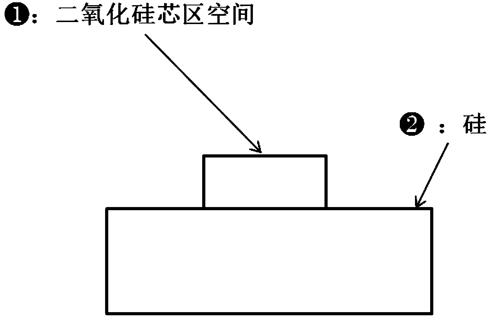
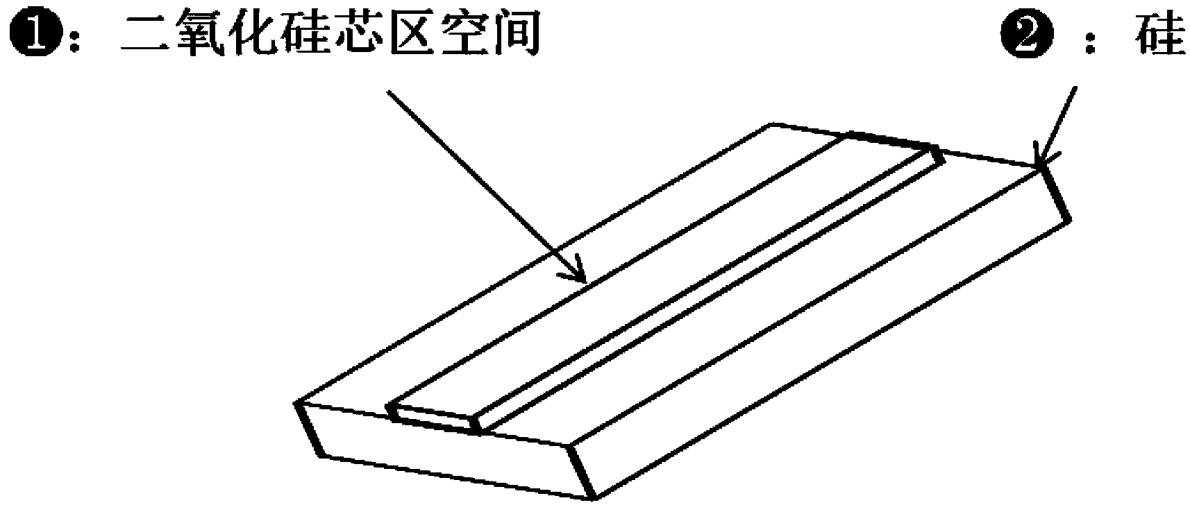
[0037] (2) Micro-etching silicon dioxide on a silicon-based wafer to create a waveguide core space;

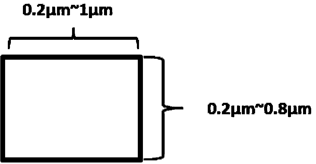
[0038] (3) The thickness of the silicon dioxide layer is 0.2 μm to 2 μm;

[0039] (4) The refractive index of silicon is 3.42, and that of silicon dioxide is 1.444...


PUM


Abstract

The invention belongs to the technical field of optical material devices, and particularly relates to a silicon-based silicon dioxide waveguide, and manufacturing and application methods thereof. With the adoption of the silicon-based silicon dioxide waveguide, and the manufacturing and application methods thereof, a waveguide core area space of which the cross section is rectangular is formed through carrying out a photoetching process on silicon dioxide on a silicon base in the waveguide. Specific geometrical parameters are given to a silicon-based silicon dioxide waveguide structure, various all-optical logic devices can be realized, wherein the all-optical logic devices are as follows: an all-optical divider, an all-optical coupler, an all-optical switch, an all-optical logic gate, an all-optical storage and an all-optical router which can be obtained through processing the silicon-based silicon dioxide waveguide with a specific domain structure; furthermore, the application also comprises an all-optical integrated chip and an all-optical network; and a femtosecond pulse light source of which the wavelength range is 270-1100nm is used as a high-speed input signal of the all-optical logic device. The silicon dioxide domain structure adopted by the invention has the advantages of being compatible with a silicon microelectronic process in manufacturing, and being easily popularized and applied to industries.

Description

technical field [0001] The invention belongs to the technical field of optical materials and devices, in particular to a silicon-based silicon dioxide waveguide and its manufacturing and application method. Background technique [0002] The existing materials used in all-off logic devices mainly include photonic crystals, nonlinear bistable materials, nanowires and plasmonic waveguides. The existing problems are that it is expensive, not miniaturized enough, the process is complicated, the S / N ratio is low, the contrast between the logical input and output of the optical signal "1" and "0" is small, and it even needs to be operated in a low temperature environment, so it is difficult to popularize in practical applications. [0003] Silicon material is the cornerstone of the modern microelectronics industry, and its processing technology is mature, making most of the semiconductor chips. [0004] It is a very mature and standard process to generate a thin layer of silicon d...

Claims


Application Information

Patent Timeline
Patent Type & Authority Applications(China)
IPC IPC(8): G02B6/122G02B6/13
Inventor 张小平单欣岩李铭晖张卫华
Owner TSINGHUA UNIV
Why Eureka
Try Eureka