Double photoresist structure and its processing method
A processing method and photoresist technology, applied in optics, optomechanical equipment, photosensitive materials for optomechanical equipment, etc., can solve the problem of poor pattern transfer fidelity, and achieve the effect of improving fidelity
- Summary
- Abstract
- Description
- Claims
- Application Information
AI Technical Summary
Problems solved by technology
Method used
Image

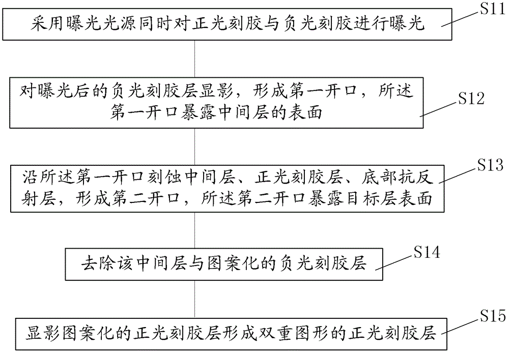
Examples
Embodiment 1
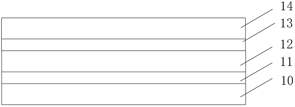
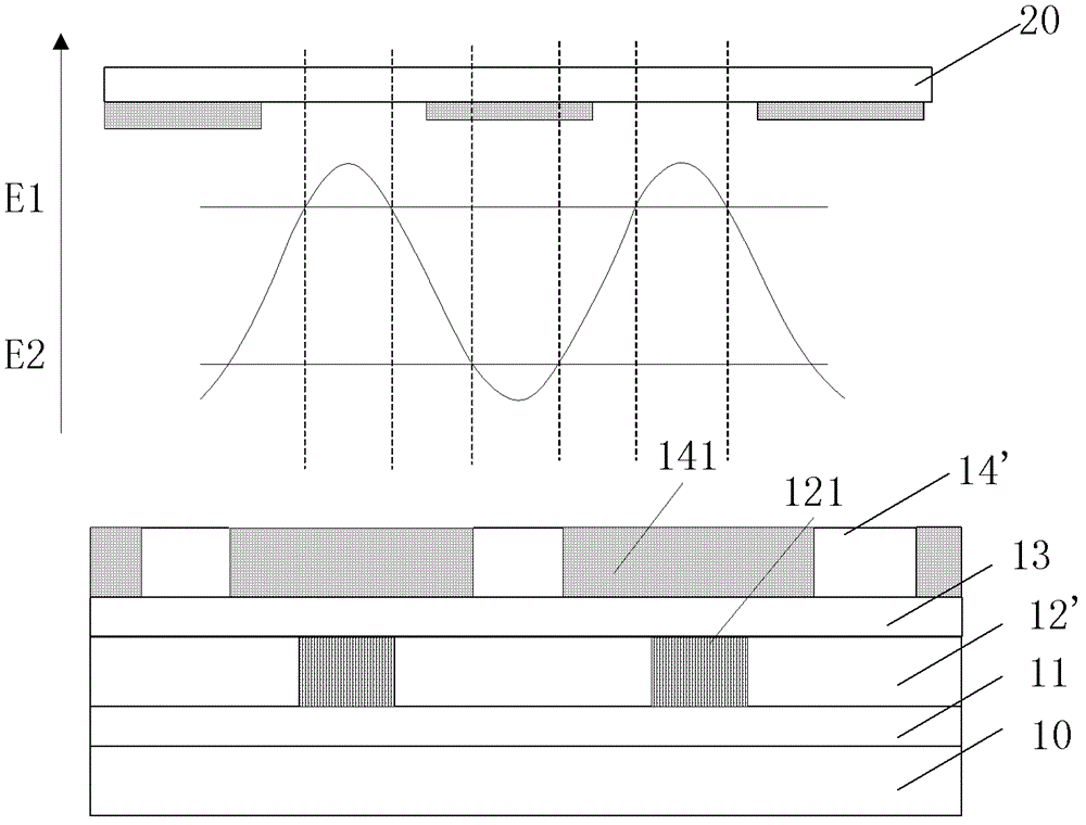
[0038] refer to figure 1As shown, the double photoresist provided in the first embodiment is formed on the target layer 10, and the double photoresist is sequentially as follows from bottom to top: bottom antireflection layer (BARC) 11, positive photoresist layer 12, intermediate layer 13 and negative photoresist layer 14 . The bottom anti-reflection layer 11 is used to increase the intensity of bottom light in the exposure process, and the material can be selected from existing BARC materials, and can be an organic anti-reflection coating or an inorganic anti-reflection coating.
[0039] The inorganic antireflection coating is made of, for example, titanium (titanium), titanium oxide (titanium oxide), titanium nitride (titanium nitride), chromium oxide (chromium oxide), carbon (carbon), amorphous silicon (amorphous silicon), nitrogen Silicon nitride (silicon nitride), silicon nitride oxide (silicon nitride oxide), silicon carbon oxide (silicon carbon oxide) and other materia...
Embodiment 2
[0064] The structure and processing method of the double photoresist provided in the second embodiment and the first embodiment are roughly the same, the only difference is that the double photoresist on the target layer 10 is sequentially from bottom to top: bottom anti-reflection layer (BARC) 11. Negative photoresist layer, intermediate layer and silicon-containing water-soluble positive photoresist layer. Wherein, the material selection of each layer of the negative photoresist layer, the intermediate layer and the silicon-containing water-soluble positive photoresist layer is the same as that of the first embodiment. The bottom anti-reflection layer 11 is an optional layer, which is used to increase the intensity of bottom light in the exposure process, and the material can be selected from existing BARC materials.
[0065]Aiming at the differences between the second embodiment and the first embodiment, the processing method of the double photoresist structure in the secon...
PUM
| Property | Measurement | Unit |
|---|---|---|
| Thickness | aaaaa | aaaaa |
Abstract
Description
Claims
Application Information
 - Generate Ideas
- Intellectual Property
- Life Sciences
- Materials
- Tech Scout
- Unparalleled Data Quality
- Higher Quality Content
- 60% Fewer Hallucinations
Browse by: Latest US Patents, China's latest patents, Technical Efficacy Thesaurus, Application Domain, Technology Topic, Popular Technical Reports.
© 2025 PatSnap. All rights reserved.Legal|Privacy policy|Modern Slavery Act Transparency Statement|Sitemap|About US| Contact US: help@patsnap.com