
Transconductance operational amplifier

An operational amplifier and transconductance technology, used in differential amplifiers, improved amplifiers to expand bandwidth, DC-coupled DC amplifiers, etc., can solve the problems of complex auxiliary amplifier circuit structure, high power consumption, etc. good effect of power consumption and frequency characteristics

Active Publication Date: 2013-10-23
SHANGHAI HUAHONG GRACE SEMICON MFG CORP
View PDF5 Cites 6 Cited by
  • Summary
  • Abstract
  • Description
  • Claims
  • Application Information

AI Technical Summary

Problems solved by technology

However, the structure of the auxiliary amplifier circuit of the existing gain bootstrap operational amplifier is complicated, it has multiple biases, and the power consumption is large

Method used


Image

  • Transconductance operational amplifier
  • Transconductance operational amplifier
  • Transconductance operational amplifier

Examples


Embodiment Construction

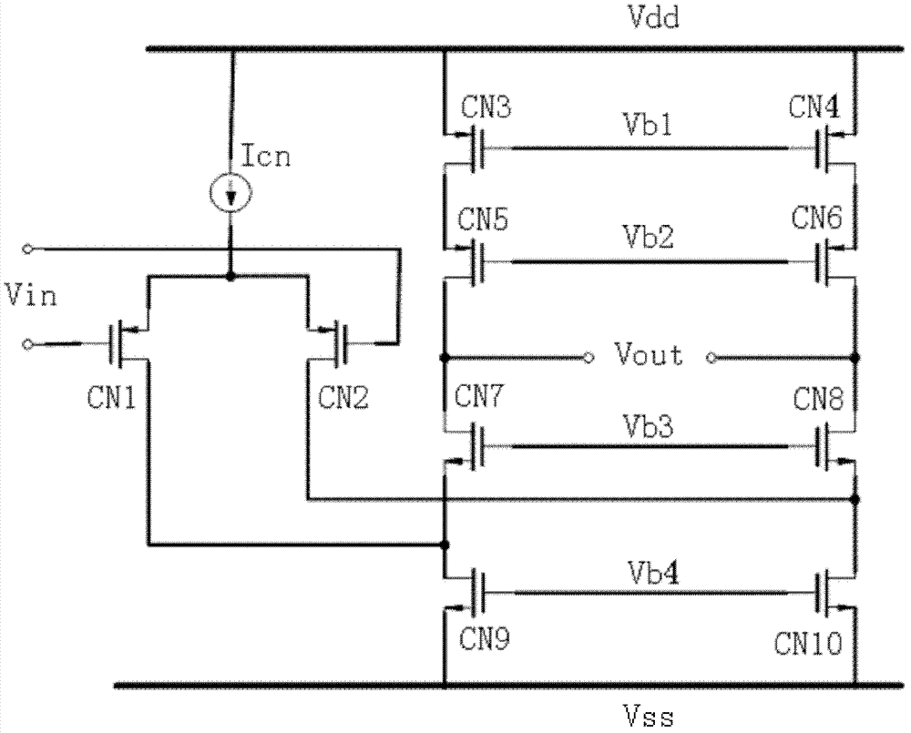
[0021] like Figure 4 As shown, it is a circuit diagram of a transconductance operational amplifier according to an embodiment of the present invention; the transconductance operational amplifier according to the embodiment of the present invention includes:

[0022] The first NMOS transistor M1 and the second NMOS transistor M2, the gates of the first NMOS transistor M1 and the second NMOS transistor M2 serve as the input ends of a pair of differential input signals of the transconductance operational amplifier; the first NMOS transistor The sources of the transistor M1 and the second NMOS transistor M2 are connected to the drain of the ninth NMOS transistor M9; the source of the ninth NMOS transistor M9 is grounded, and the gate of the ninth NMOS transistor M9 is connected to the ground. the first bias voltage VN1.

[0023] The third NMOS transistor M3, the fourth NMOS transistor M4, the fifth PMOS transistor M5 and the sixth PMOS transistor M6, the source of the third NMOS...


PUM


Abstract

The invention discloses a transconductance operational amplifier capable of signal differential inputting and signal differential outputting. The transconductance operational amplifier adopts a gain-boosted manner and comprises a single-transistor structure of a pair of PNMOS and NMOS. Each single structure is provided with an auxiliary amplifier. According to the transconductance operational amplifier, the auxiliary amplifier technique of the single transistor is adopted, gain of the transconductance operational amplifier is increased through increasing output impedance of the entire amplifier, so that the purpose of increasing the transconductance operational amplifier gain can be achieved. Meanwhile, an auxiliary amplifier circuit of the transconductance operational amplifier is compared with that of an existing structure, the transconductance operational amplifier is simple in structure and easy to realize, multipath biasing of the auxiliary amplifier is reduced, power can be reduced, frequency feature is good, and capabilities of high speed and wide broadband can be realized.

Description

technical field [0001] The present invention relates to a semiconductor integrated circuit, in particular to a transconductance operational amplifier. Background technique [0002] High-gain transconductance operational amplifiers are widely used in CMOS analog integrated circuits. In order to obtain high gain, the commonly used structures are two-stage operational amplifiers and operational amplifiers with gain bootstrapping techniques. Since the frequency compensation technology is inevitably used in the two-stage operational amplifier, the bandwidth of the operational amplifier with this structure is small. Operational amplifiers using gain bootstrap technology include differential circuits and cascode bootstrap circuits. The differential circuits are divided into NMOS transistors, namely N-channel MOS field effect transistors and PMOS transistors. P-channel MOS field effect transistor There are two structures, in which the differential circuit adopts the gain bootstrap...

Claims


Application Information

Patent Timeline
Patent Type & Authority Applications(China)
IPC IPC(8): H03F3/45H03F1/42
Inventor 朱红卫唐敏刘燕娟刘国军
Owner SHANGHAI HUAHONG GRACE SEMICON MFG CORP
Learn More