Insulated gate bipolar transistor and manufacturing method thereof

A technology of bipolar transistors and manufacturing methods, applied in semiconductor/solid-state device manufacturing, semiconductor devices, electrical components, etc., can solve the problems of low power density, small size, high saturation voltage drop, etc., and achieve improved cut-off rate and lower cut-off The effect of breaking loss and good ohmic contact

Inactive Publication Date: 2013-10-30
上海永电电子科技有限公司
View PDF5 Cites 5 Cited by
  • Summary
  • Abstract
  • Description
  • Claims
  • Application Information

AI Technical Summary

Problems solved by technology

[0005] The traditional IGBT structure is mainly planar gate and trench gate, but no matter which structure, it is necessary to select a high resistivity and a very thick epitaxial layer or substrate to obtain a large withstand voltage, resulting in a high saturation voltage drop , the power density is low. With the requirements of the new generation of devices for junction temperature and power density, the thickness of the IGBT needs to be made thinner and the size smaller. Currently, it mainly relies on the introduction of field stop (Field Stop, referred to as "FS") In addition, in the switching application of the standard half-bridge circuit, the IGBT must be connected in reverse parallel with an external fast recovery diode FRD to form a small module, and the two small modules are connected in series to form a half-bridge circuit, respectively are the upper half bridge and the lower half bridge, and the upper half bridge is connected in parallel with the inductive load

Method used


Image

  • Insulated gate bipolar transistor and manufacturing method thereof
  • Insulated gate bipolar transistor and manufacturing method thereof
  • Insulated gate bipolar transistor and manufacturing method thereof

Examples


Embodiment Construction

[0032] In the following description, many technical details are proposed in order to enable readers to better understand the application. However, those skilled in the art can understand that without these technical details and various changes and modifications based on the following implementation modes, the technical solution claimed in each claim of the present application can be realized.

[0033] In order to make the purpose, technical solution and advantages of the present invention clearer, the following will further describe the implementation of the present invention in detail in conjunction with the accompanying drawings.

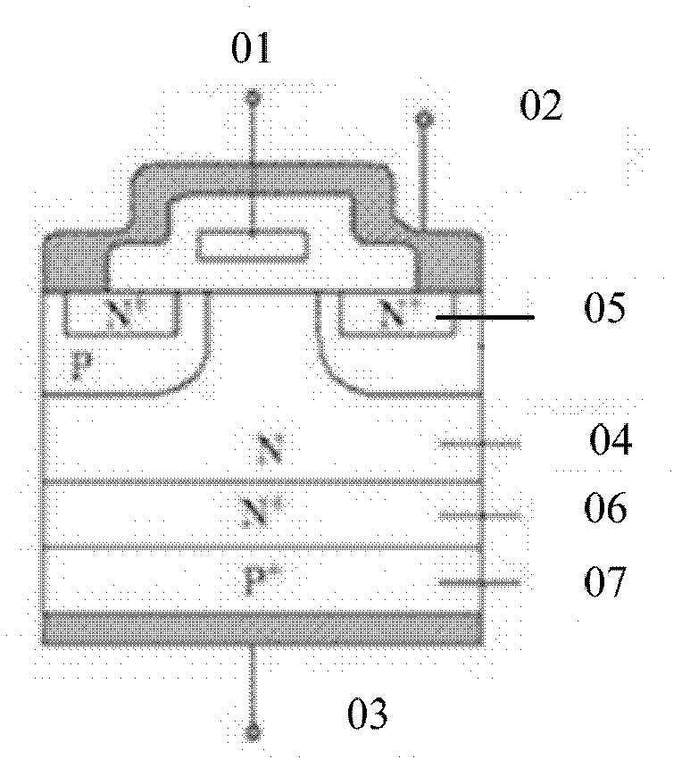
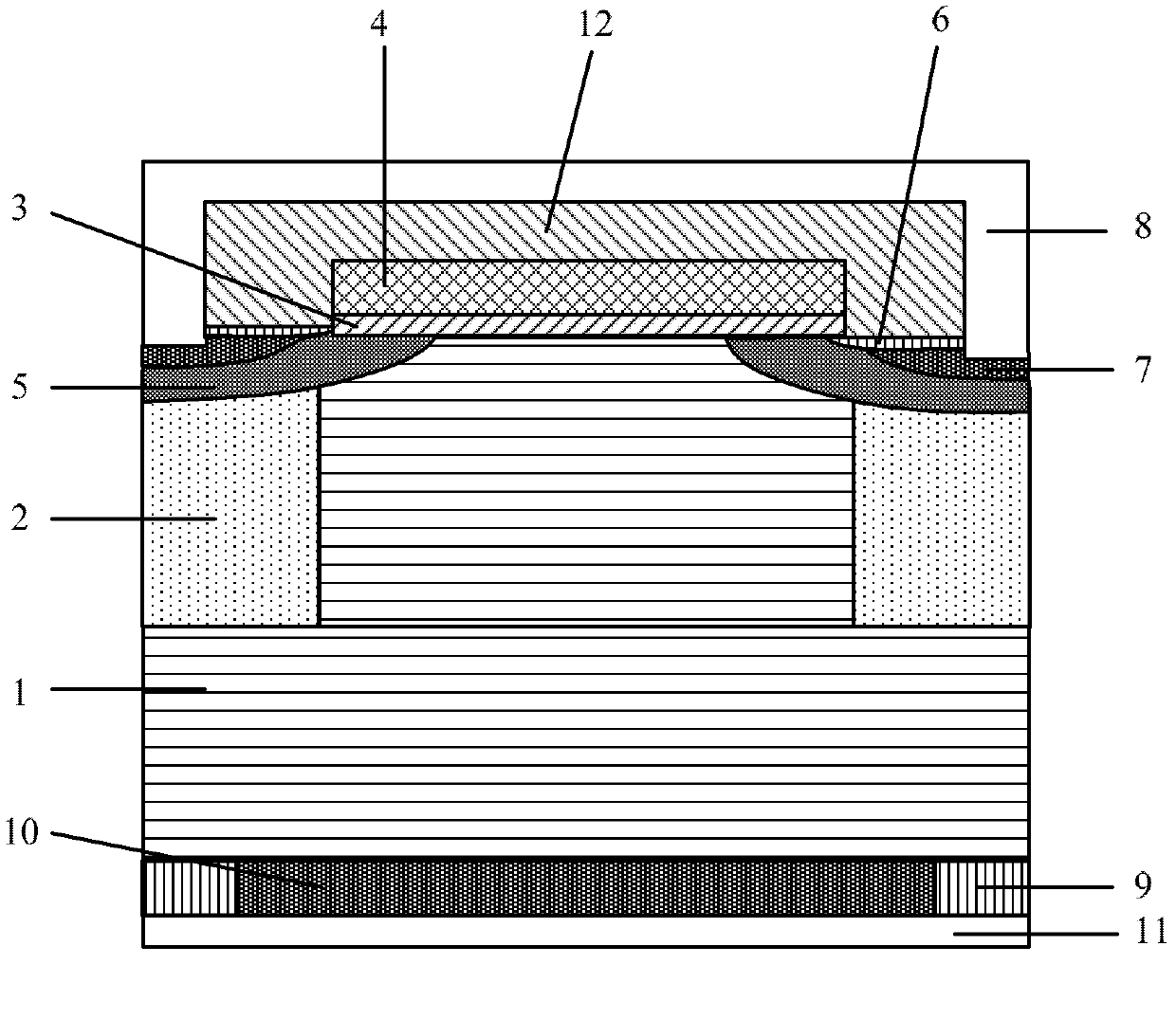
[0034] The first embodiment of the present invention relates to an IGBT. figure 2 is a schematic diagram of the structure of the insulated gate bipolar transistor.

[0035] Specifically, as figure 2 as shown,

[0036] The insulated gate bipolar transistor is on one side of the substrate 1 of the first semiconductor type, between the substrate...


PUM


Abstract

The invention relates to the field of electronic devices, and discloses an insulated gate bipolar transistor and a manufacturing method thereof. According to the insulated gate bipolar transistor and the manufacturing method thereof, a first doping region is used as a super junction in the insulated gate bipolar transistor, internal fast recovery diodes are formed in a channel region and a second doping region, the advantages of a super junction MOS and the advantages of a reverse conducting insulated gate bipolar transistor are combined, the saturation voltage drop of the insulated gate bipolar transistor can be effectively lowered, higher power density is achieved, and meanwhile due to the fact that the fast recovery diodes are removed in module packaging process, production cost can be effectively lowered. Due to a buffer region layer, the requirement for the thickness of a substrate is lowered, the buffer region layer is used for accelerating the composite process of charge carriers, the trailing time of insulated gate bipolar transistor products can be effectively shortened, the turn-off loss of the products is reduced, and the cut-off frequency of the products is increased.

Description

technical field [0001] The invention relates to the field of electronic devices, in particular to an insulated gate bipolar transistor. Background technique [0002] Insulated Gate Bipolar Transistor (Insulated Gate Bipolar Transistor, referred to as "IGBT") is composed of Bipolar Junction Transistor (Bipolar Junction Transistor, referred to as "BJT") and Metal-Oxide-Semiconductor (Metal-Oxide-Semiconductor, referred to as "MOS") Composite fully-controlled voltage-driven power semiconductor devices. The saturation voltage of BJT is lowered, the carrying current density is large, but the driving current is large; the driving power of MOS is small, the switching speed is fast, but the conduction voltage drop is large, and the current carrying density is small. IGBT combines the advantages of the above two devices, the driving power is small and the saturation voltage is low, and it is very suitable for the conversion system with a DC voltage of 600V and above, such as AC moto...

Claims


Application Information

Patent Timeline
Patent Type & Authority Applications(China)
IPC IPC(8): H01L29/739H01L21/331
Inventor 吴多武陶凯孙军时以成
Owner 上海永电电子科技有限公司
Why Eureka
Try Eureka