[0002] In recent years, due to the characteristics of high power conversion efficiency and
high power density of the LLC series resonant converter (LLC resonant power converter), it has been widely used in various electronic products in the industry. However, the LLC series resonant converter cannot More and more attention has been paid to the defect of
light load regulation
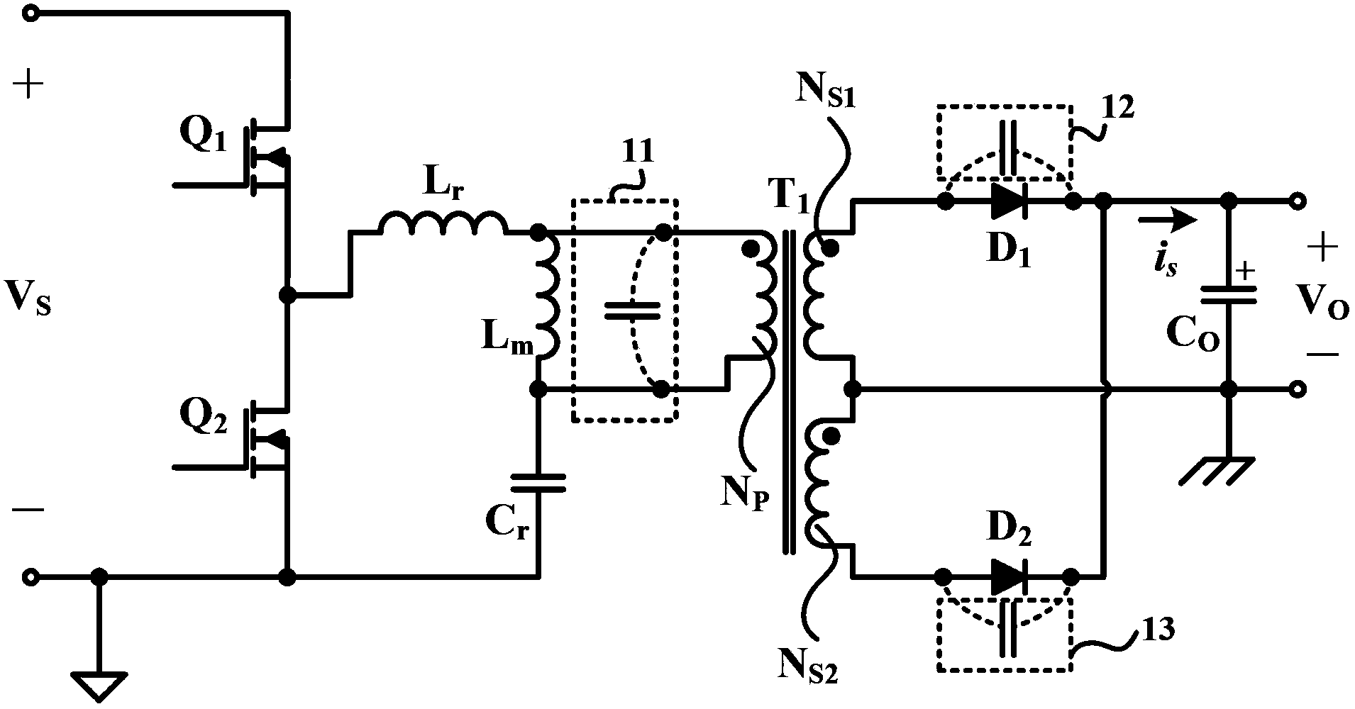
[0003] As an example of a conventional LLC series resonant converter and its description in a paper by Jin-Tae Kim published in the March 2011 edition of "NEWELECTRONICS" journal, see figure 1 As shown, the main reason why the LLC series resonant converter cannot achieve light load
voltage regulation is that its primary winding N p The parasitic
capacitance 11 (parasitic
capacitance) of the
secondary side and the parasitic
capacitance 12, 13 of the two rectifiers (rectifiers) on the full-wave rectification circuit (full-wave rectification circuit) of the
secondary side, at the switching moment of the power switch, the parasitic capacitance is inevitably will be with the resonant inductor L r
Resonance is generated, so that
excess energy will accumulate on the parasitic capacitance, and this energy will greatly increase the voltage
gain of the LLC series resonant converter under light load conditions, thereby causing the LLC series The resonant converter cannot convert the output voltage V o changes, effectively regulating within a designed range
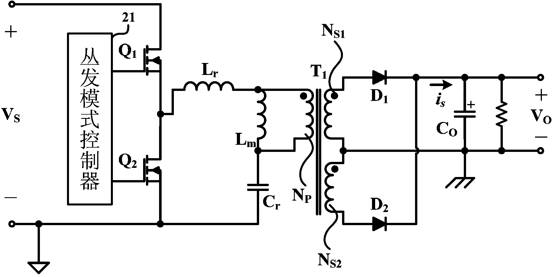
[0004] In view of this, Jin-Tae Kim also mentioned in the aforementioned paper that two traditional methods can be used to solve the aforementioned problem that light
load regulation cannot be achieved, see figure 2 As shown, the first approach is to install a burst mode controller (burst mode controller) 21 on the primary side of the LLC series resonant converter to control the two power switches Q on the primary side 1 , Q 2 , providing a burst
mode control, the control method forces the LLC series resonant converter to operate intermittently under light load conditions, in the hope that the LLC series resonant converter can operate within the generated output voltage V o When it is about to be equal to the upper
limit value (upper limited value) of a designed output voltage (designed output voltage), stop operating, and the output voltage V generated o When it is about to be equal to the
lower limit value of the output voltage of the design (lower limited value), it starts to operate. Although, this method can also achieve the output voltage V o Variations, regulated (regulated) within a design range, however, due to the
burst frequency (
burst frequency) designed in the burst mode controller 21, in addition to including the power switches Q 1 , Q 2 In addition to the switching period (switching period), it also includes a stopped period (stopped period), so that when the LLC series resonant converter operates at the
burst frequency, a series of noises close to the
audio frequency will be generated. This annoying
noise does cause a certain degree of
noise pollution to the surrounding environment of the LLC series resonant converter
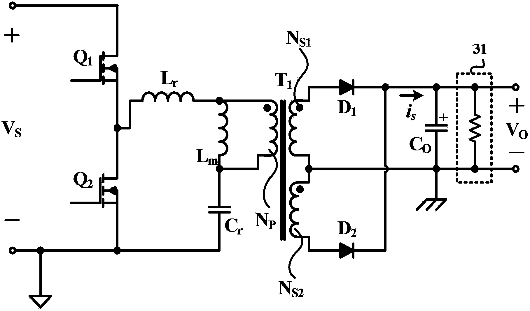
[0005] refer to image 3 As shown, another approach mentioned by Jin-Tae Kim in the aforementioned paper is to install a dummy
resistor 31 on the secondary side of the LLC series resonant converter, and the
dummy load 31 is connected in parallel The secondary side output
capacitor C o , thereby increasing the load to prevent the LLC series resonant converter from operating at a light load state, thereby achieving a control on the output voltage V o However, this method, in addition to causing the power conversion efficiency of the LLC series resonant converter to be poor, is still under light load (such as: standby state), resulting in
higher power due to the
dummy load 31 consume
[0006] According to the above, under the premise of maintaining the existing power conversion efficiency and avoiding annoying
noise, the above two methods mentioned by Jin-Tae Kim cannot make the LLC series resonant converter to output voltage V o Changes to effectively achieve the purpose of light load
voltage regulation[0007] In view of this, Y.Q.Ye, Chao Yan, J.H.Zeng and J.P.Ying were also mentioned in a paper titled "A Novel
Light Load Solution for LLC Series
Resonant Converter" published in the IEEE journal in 2007 , under light load conditions, the LLC series resonant converter cannot effectively regulate the output voltage V o The reason for the change is also due to the parasitic capacitance on the primary winding and the two rectifiers on the secondary side, and at the switching moment of the power switch, the parasitic capacitance will inevitably interact with the resonant inductor L r
Resonance is generated, so that
excess energy is accumulated on the parasitic capacitance, the solution that the four people think about, refer to Figure 4 Shown, are the two rectifiers D on the secondary side of the LLC series resonant converter 1 、D 2 Add a parallel secondary recharging circuit (secondary recharging circuit) 41, 42 respectively, in order to make the primary winding N p When the
excess energy accumulated on the parasitic capacitance of the device is transferred to the secondary side, it can be recharged to the primary side through the secondary recharging circuits 41, 42. Although, this solution can also achieve the output voltage V o The purpose of adjusting the change within a design range, however, since it is necessary to use an external
driving circuit (external
driving circuit) (not shown in the figure), the switches Q in the secondary recharging circuits 41, 42 a1 , Q a2 switching control, and the relevant control signals generated by the external drive circuit must depend on the power switches Q on the primary side A , Q B , Q C , Q D Therefore, not only will the overall
circuit complexity and production cost of the LLC series resonant converter increase greatly, but also due to the multiplication of calculation data and programs, it will inevitably cause the
transmission delay of related control signals (
propagation delay), and then As a result, the secondary recharging circuits 41 and 42 cannot immediately recharge the obtained excess energy to the primary side, and finally, it is still unable to effectively regulate the output voltage V under light load conditions. o The change

