Method for manufacturing grid lines with high uniformity through double exposure

A gate line, double exposure technology, applied in microlithography exposure equipment, photolithographic process exposure devices, optics, etc., can solve the problems of low production capacity, high cost, limited uniformity, etc.

Active Publication Date: 2013-11-20
SHANGHAI HUALI MICROELECTRONICS CORP
View PDF6 Cites 8 Cited by
  • Summary
  • Abstract
  • Description
  • Claims
  • Application Information

AI Technical Summary

Problems solved by technology

[0008] However, the process of the above scheme is relatively complicated, the

Method used


Image

  • Method for manufacturing grid lines with high uniformity through double exposure
  • Method for manufacturing grid lines with high uniformity through double exposure
  • Method for manufacturing grid lines with high uniformity through double exposure

Examples


Embodiment Construction

[0043] In order to make the content of the present invention clearer and easier to understand, the content of the present invention will be described in detail below in conjunction with specific embodiments and accompanying drawings.

[0044] Figure 4A to Figure 4G A method for fabricating gate lines with high uniformity by double exposure according to a preferred embodiment of the present invention is schematically shown.

[0045] Specifically, as Figure 4A to Figure 4G As shown, the method for making gate lines with high uniformity by double exposure according to a preferred embodiment of the present invention includes:

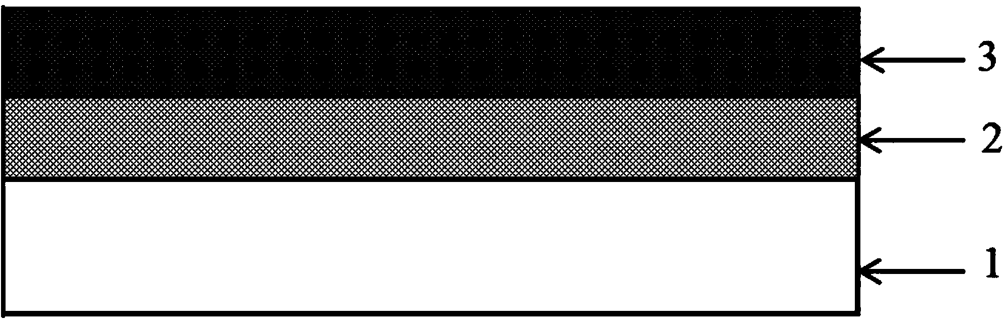
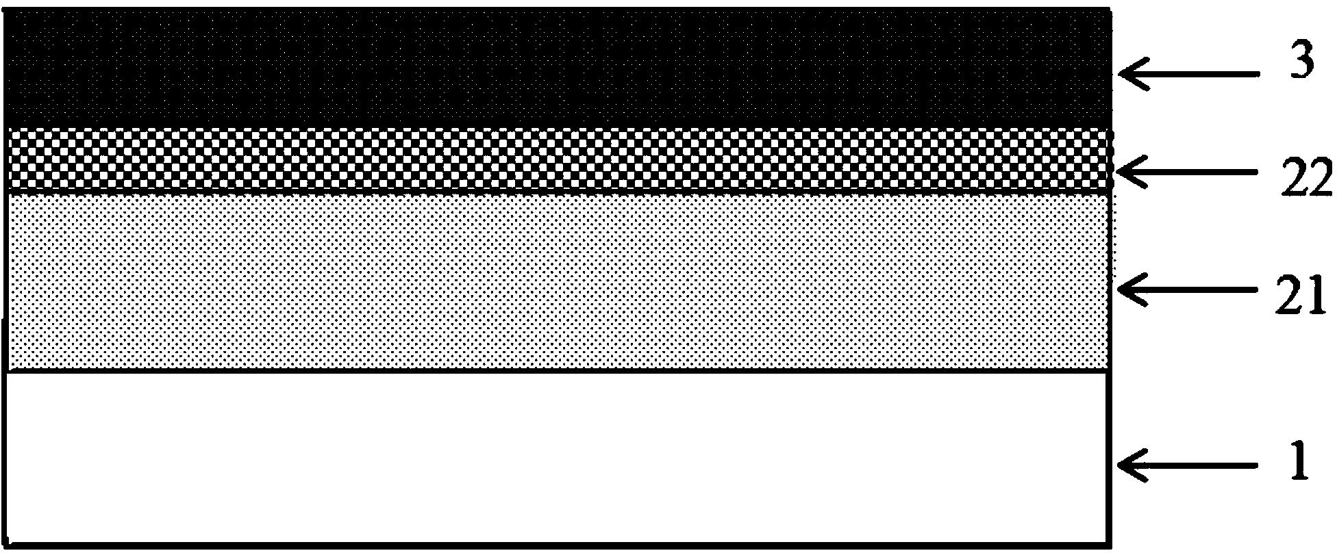
[0046] The first step: sequentially deposit polysilicon film 4, amorphous carbon film 21, and carbon-containing silicon oxide film 22 on substrate silicon wafer 1, and then coat the first photoresist 3 of formable hard film, such as Figure 4A shown.

[0047] Preferably, the thickness of the amorphous carbon film 21 is 20 nm to 300 nm, more preferably,...


PUM

PropertyMeasurementUnit
Thicknessaaaaaaaaaa
Thicknessaaaaaaaaaa
Thicknessaaaaaaaaaa

Abstract

A method for manufacturing grid lines with high uniformity through double exposure comprises the following steps: depositing a polycrystalline silicon film, an amorphous carbon film and a carbonaceous silicon oxide film and coating a first photoresist; carrying out exposure and development to form a first grid line structure in the films of the first photoresist; coating alkyl-amino solidification materials to solidify the first grid line structure in the first photoresist, heating to enable solidification materials and the surface of the first photoresist to react, so as to form isolation films undissolved in a second photoresist, and removing residual solidification materials; coating the second photoresist; forming a first line end cutting pattern in second photoresist films; etching the isolation films and first grid lines to form a second line end cutting pattern, and then removing the second photoresist; etching the carbonaceous silicon oxide film, the amorphous carbon film and the polycrystalline silicon film in sequence by taking the residual isolation films and the first grid lines as masks, and removing the residual carbonaceous silicon oxide film and the amorphous carbon film, so as to form a second grid line structure on a polycrystalline silicon film layer.

Description

technical field [0001] The invention relates to the field of semiconductor manufacturing, and more specifically, the invention relates to a method for manufacturing high-uniformity gate lines by double exposure. Background technique [0002] As the integration level of semiconductor chips continues to increase, the feature size of transistors continues to shrink, posing more and more challenges to the photolithography process. The traditional photolithography process usually adopts organic bottom anti-reflective coating (BARC) with polymer materials as the main body to improve the capability of the photolithography process. Figure 1A It is a schematic diagram of the structure of the substrate silicon wafer 1, the organic anti-reflection film 2, and the photoresist 3. The organic anti-reflection film can also expand the adjustable range of the etching process and improve the uniformity of the pattern structure after etching. [0003] After entering the 45nm technology node,...

Claims


Application Information

Patent Timeline
IPC IPC(8): H01L21/28H01L21/3213H01L21/027G03F7/00G03F7/20
Inventor 毛智彪
Owner SHANGHAI HUALI MICROELECTRONICS CORP
Why Eureka
Try Eureka