Three-dimensional semiconductor device on insulator and forming method of three-dimensional semiconductor device

A semiconductor and insulator technology, applied in the field of three-dimensional semiconductor devices on insulators and their formation, can solve the problems of expensive UTBSOI wafers, and achieve the effects of large-scale production, easy implementation, and simple process

Active Publication Date: 2013-11-20
TSINGHUA UNIV
View PDF3 Cites 5 Cited by
  • Summary
  • Abstract
  • Description
  • Claims
  • Application Information

AI Technical Summary

Problems solved by technology

So, producing UTBSOI wafers is very expensive
At present, FinFET devices and UTB SOI MOS devices seem to be competing technologies running on two parallel tracks, and each continues to develop along its own technical route, and has not yet been well integrated

Method used


Image

  • Three-dimensional semiconductor device on insulator and forming method of three-dimensional semiconductor device
  • Three-dimensional semiconductor device on insulator and forming method of three-dimensional semiconductor device
  • Three-dimensional semiconductor device on insulator and forming method of three-dimensional semiconductor device

Examples


Embodiment Construction

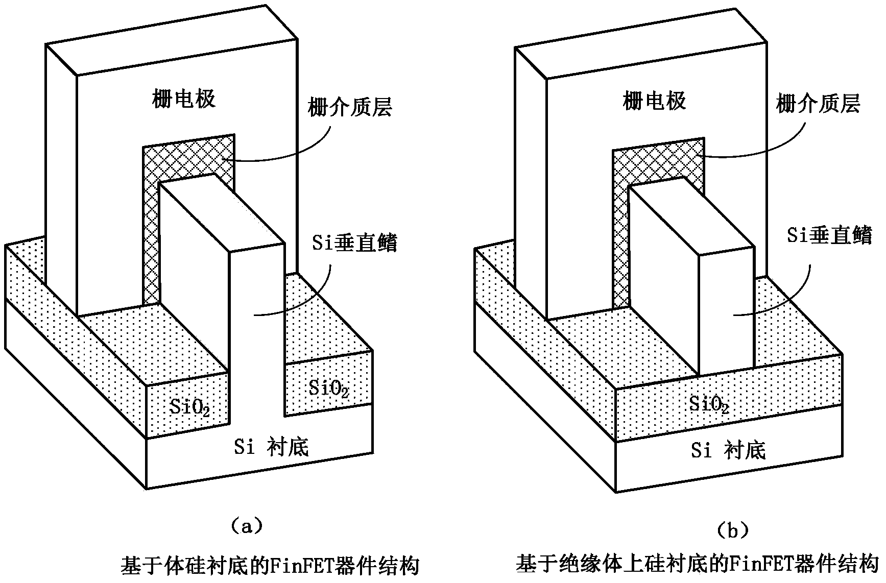
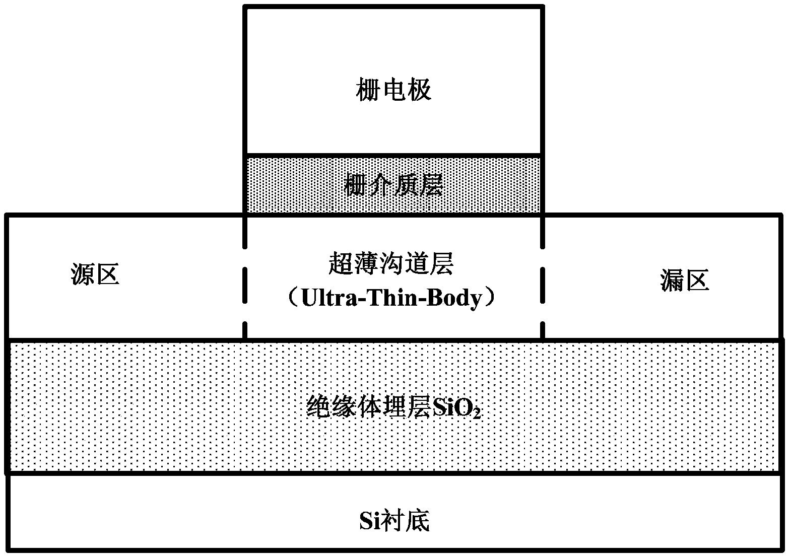
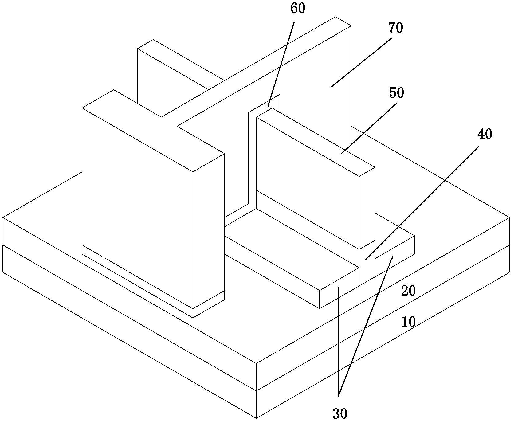
[0044] Embodiments of the present invention are described in detail below, examples of which are shown in the drawings, wherein the same or similar reference numerals designate the same or similar elements or elements having the same or similar functions throughout. The embodiments described below by referring to the figures are exemplary and are intended to explain the present invention and should not be construed as limiting the present invention.

[0045] In describing the present invention, it should be understood that the terms "center", "longitudinal", "transverse", "length", "width", "thickness", "upper", "lower", "front", " Orientation or position indicated by "back", "left", "right", "vertical", "horizontal", "top", "bottom", "inner", "outer", "clockwise", "counterclockwise", etc. The relationship is based on the orientation or positional relationship shown in the drawings, and is only for the convenience of describing the present invention and simplifying the descrip...


PUM


Abstract

The invention discloses a three-dimensional semiconductor device on an insulator and a forming method of the three-dimensional semiconductor device. The device comprises a substrate, an ultra-thin insulation layer, a plane ultra-thin semiconductor structure, an insulation fin-shaped seed layer, a vertical semiconductor fin, a grid dielectric layer and a grid electrode, wherein the ultra-thin insulation layer is made of single crystal rare earth oxide or single crystal beryllium oxide, the plane ultra-thin semiconductor structure has the first width and the second width, and is positioned above the ultra-thin insulation layer, the insulation fin-shaped seed layer has the second width and the second height, is embedded in the plane ultra-thin semiconductor structure and is in adjacent joint with the upper surface of the ultra-thin insulation layer, the second width is smaller than the first width, the second height is greater than or equal to the first height, the insulation fin-shaped seed layer is made of single crystal rare earth oxide or single crystal beryllium oxide, the vertical semiconductor fin has the third width and the third height, and is positioned above the insulation fin-shaped seed layer, and in addition, the third width is smaller than the first width. The three-dimensional semiconductor device has the advantages that the driving current is great and can be continuously regulated, the process compatibility is realized, and the qualification rate is high.

Description

technical field [0001] The invention belongs to the technical field of semiconductor manufacturing, and in particular relates to a three-dimensional semiconductor device on an insulator and a forming method thereof. Background technique [0002] Metal-oxide-semiconductor field-effect transistors (MOSFETs) have served the integrated circuit industry for over forty years. People have invented a variety of ingenious techniques to make the feature size shrink continuously, but it has not changed its basic structure. However, the integrated circuit design window, including performance, dynamic power consumption, static power consumption, and device tolerances, has shrunk to the point where a new transistor structure has to be invented. [0003] As the gate length continues to shrink, the transfer characteristics of the MOSFET (I ds -V gs ) degenerates mainly in two aspects. One is that the subthreshold slope becomes larger and the threshold voltage decreases, that is, by redu...

Claims


Application Information

Patent Timeline
Patent Type & Authority Applications(China)
IPC IPC(8): H01L29/78H01L29/786H01L29/423H01L29/51H01L27/12H01L21/336
CPCH01L29/7853
Inventor 梁仁荣王敬许军
Owner TSINGHUA UNIV
Why Eureka
Try Eureka