High-gain AlGaN ultraviolet avalanche photodetector and preparation method thereof

A photodetector, ultraviolet avalanche technology, applied in circuits, electrical components, semiconductor devices, etc., can solve the problem of slow development of APD, and achieve the effect of improving APD avalanche multiplication factor and reducing applied voltage and dark current.

Inactive Publication Date: 2013-11-20
NANJING UNIV
View PDF5 Cites 26 Cited by
  • Summary
  • Abstract
  • Description
  • Claims
  • Application Information

AI Technical Summary

Problems solved by technology

AlGaN and GaN have similar material properties. Although the development of GaN APD has made gratifying progress, however, the APD of AlGaN materials has developed slowly. In 2007, Turgut et al. reported again that the Al compositio

Method used


Image

  • High-gain AlGaN ultraviolet avalanche photodetector and preparation method thereof
  • High-gain AlGaN ultraviolet avalanche photodetector and preparation method thereof
  • High-gain AlGaN ultraviolet avalanche photodetector and preparation method thereof

Examples


Embodiment 1

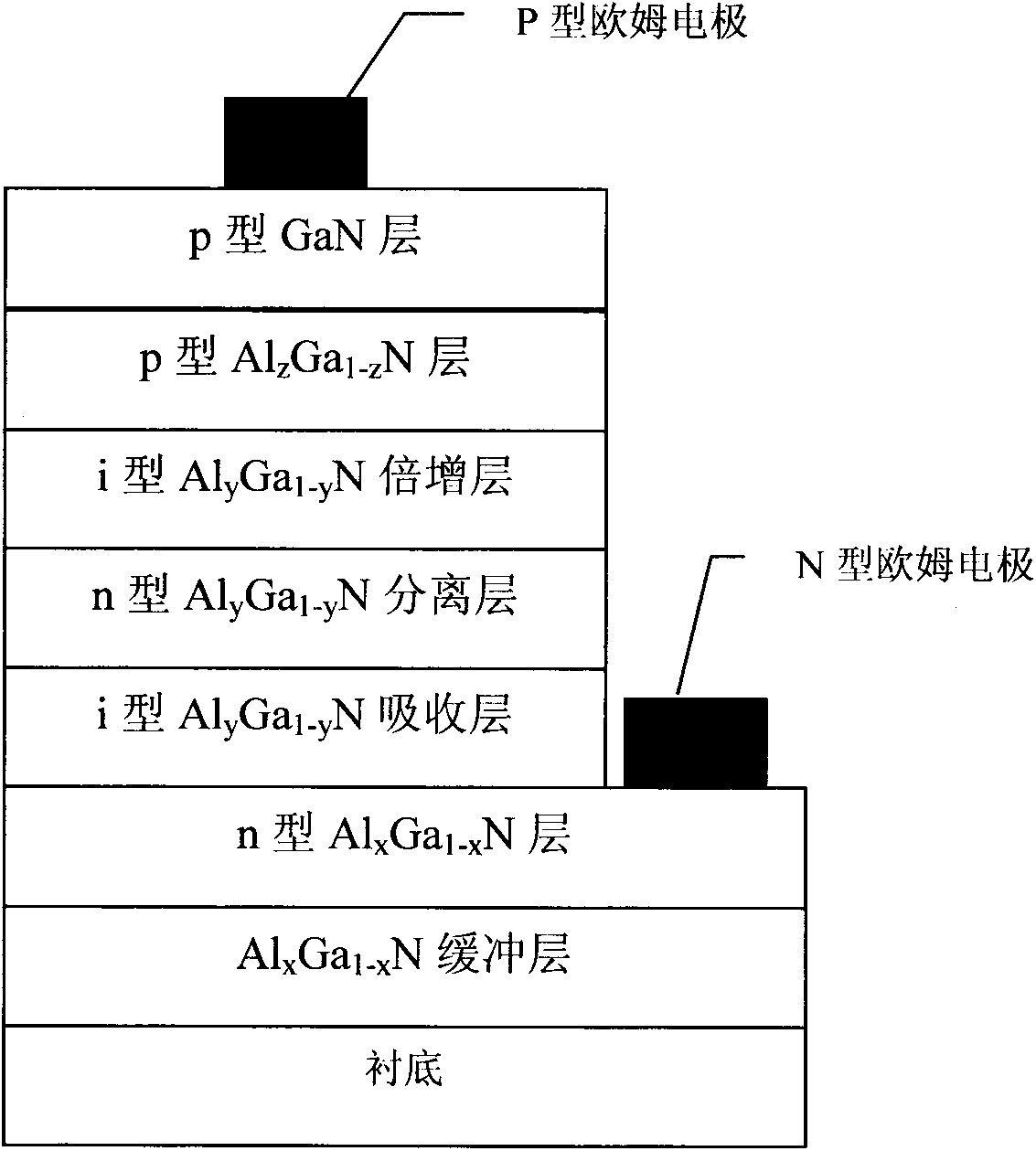
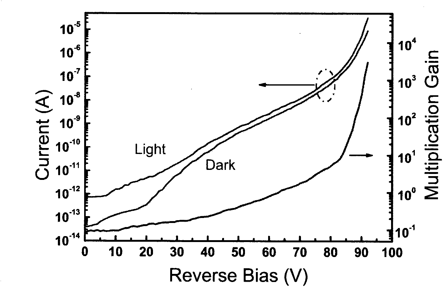
[0043] The steps of this embodiment are basically the same as those of Comparative Example 1, the difference being that the p-type Al z Ga 1-z The composition of the N layer is z=0.2, and the thickness of the P-type GaN layer is 34 nm. Figure 4 For the high-gain AlGaN ultraviolet avalanche photodetector of this embodiment, the incident light wavelength is 275nm, and the incident light power is 0.01mW / cm 2 Under the test conditions of , the photocurrent, dark current and avalanche multiplication factor obtained under different reverse bias voltages, and figure 2 It can be seen from the comparison that the p-type Al 0.2 Ga 0.8 N layer due to the i-type Al 0.4 Ga 0.6 The polarized electric field in the same direction as the external electric field is introduced into the N multiplication layer, which can significantly reduce the avalanche breakdown voltage of the APD, reduce the dark current during avalanche breakdown, and significantly increase the APD avalanche multiplica...

Embodiment 2

[0045] The steps of this embodiment are basically the same as those of Comparative Example 1, the difference being that the Al x Ga 1-x The thickness of the N buffer layer is 300nm, the n-type Al x Ga 1-x N layer thickness is 300nm, the i-type Al y Ga 1-y The thickness of the N absorbing layer is 150nm, the n-type Al y Ga 1-y The thickness of the N separation layer is 60nm, the i-type Al y Ga 1-y N multiplication layer thickness is 150nm, the p-type Al z Ga 1-z The thickness of the N layer is 120nm, the thickness of the p-type GaN layer is 30nm, and the composition x=0.8, y=0.6, z=0.3.

Embodiment 3

[0047] The steps of this embodiment are basically the same as those of Comparative Example 1, the difference being that the Al x Ga 1-x N buffer layer thickness is 600nm, the n-type Al x Ga 1-x N layer thickness is 600nm, the i-type Al y Ga 1-y The thickness of the N absorbing layer is 180nm, the n-type Al y Ga 1-y The thickness of the N separation layer is 80nm, the i-type Al y Ga 1-y N multiplication layer thickness is 180nm, the p-type Al z Ga 1-z The thickness of the N layer is 80nm, the thickness of the p-type GaN layer is 50nm, and the composition x=0.9, y=0.8, z=0.5.

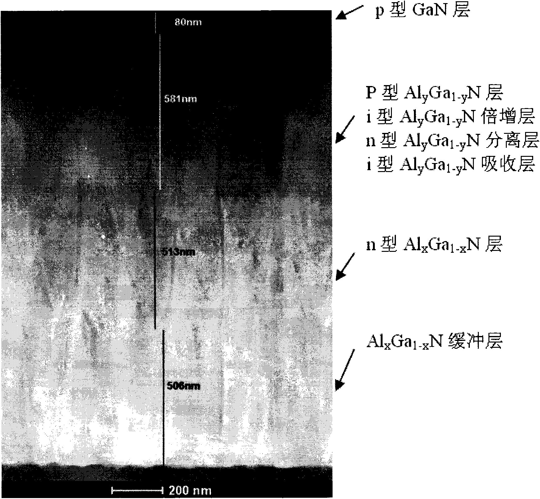
[0048] The back-incidence p-il-nl-i-n SAM type high-gain AlGaN ultraviolet avalanche photodetector is based on inserting a separation layer nl and a multiplication layer il in the traditional p-i-n structure of the same composition, while reducing the p-type layer The composition of Al, so as to achieve the purpose of improving the performance of the device. The separation layer nl separates th...


PUM

PropertyMeasurementUnit
Thicknessaaaaaaaaaa
Thicknessaaaaaaaaaa
Thicknessaaaaaaaaaa

Abstract

The invention discloses a high-gain AlGaN ultraviolet avalanche photodetector which structurally and sequentially comprises components from bottom to up: an AlN template layer, an AlxGal-xN buffer layer, an n type AlxGal-xN layer, an i type AlyGal-yN absorbing layer, an n type AlyGal-yN separating layer, an i type AlyGal-yN multiplication layer, a p type AlzGal-zN layer and a p type GaN layer, wherein an n type ohmic electrode is led out from the n type AlxGal-xN layer, a p type ohmic electrode is led out from the p type GaN layer, x is larger than y, y is larger than z, and z is larger than 0. The invention further discloses a preparation method of the high-gain AlGaN ultraviolet avalanche photodetector. The high-gain AlGaN ultraviolet avalanche photodetector adopting an SAM (security account manager) structure can obviously reduce impressed voltage and dark current during APD (avalanche photodiode) avalanche breakdown, and facilitates the increase of APD avalanche multiplication factors.

Description

technical field [0001] The patent of the present invention relates to the field of optoelectronic devices, in particular to an AlGaN ultraviolet avalanche photodetector and a preparation method thereof. Background technique [0002] Group III nitrides are semiconductor materials with wide band gap and direct band gap. They have good thermal conductivity, high electron saturation velocity, and stable physical and chemical properties. They are new semiconductor materials that have been studied at home and abroad in recent years. , high-brightness light-emitting diodes, high-power lasers and high-sensitivity solar-blind or visible light-blind photodetectors have broad application prospects. However, with the development of science and technology, people put forward higher requirements for III-nitride semiconductor materials and devices. In order to improve and enhance the photoelectric performance of III-nitride semiconductor materials and devices, people continue to dig III-ni...

Claims


Application Information

Patent Timeline
IPC IPC(8): H01L31/109H01L31/00
Inventor 陈敦军张荣郑有炓
Owner NANJING UNIV
Why Eureka
Try Eureka