Non-volatile semiconductor memory device

a semiconductor memory and non-volatile technology, applied in the direction of semiconductor devices, electrical devices, transistors, etc., can solve the problems of low power, low performance, low voltage, and conventional techniques mentioned above, and achieve the effects of reducing the applied voltage, high dielectric constant, and substantially higher heat formation

Active Publication Date: 2006-07-04
RENESAS ELECTRONICS CORP
View PDF4 Cites 12 Cited by
  • Summary
  • Abstract
  • Description
  • Claims
  • Application Information

AI Technical Summary

Benefits of technology

[0016]According to the present invention, since the second insulating film is made of high dielectric constant material, it is possible to reduce the voltage applied to the control gate at the time of the programming and the erasing. Also, even when the first insulating film is made thicker in order to prevent the leakage of charges from the charge accumulation layer, it is possible to carry out the programming and the erasing with the voltage at the same level as the conventional level. Moreover, since the second insulating film (high dielectric constant film) is made of oxide whose heat of formation is higher than that of silicon oxide, the second insulating film is stable as compared with the silicon oxide. Therefore, even when the thermal treatment is carried out at a high temperature after the formation of the second insulating film, no reaction between the second insulating film and the silicon included in the control gate occurs.
[0018]Preferably, the second insulating film is made of oxide including at least one metal selected from the group consisting of Li, Be, Mg, Al, Ca, Sc, Sr, Y, Zr, La, Hf, Ce, Pr, Nd, Sm, Eu, Gd, Tb, Dy, Ho, Er, Tm, Tb and Lu. In particular, it is further preferable that the second insulating film is made of oxide selected from the group consisting of Al2O3, CeO2, HfO2, La2O3, MgO, Sc2O3 and ZrO2. Each of these oxides has high dielectric constant, and its heat of formation is substantially higher than that of silicon oxide. It is therefore possible to reduce the applied voltage at the time of the programming and the erasing and to improve the stability with regard to the high temperature.
[0019]In another aspect of the present invention, a semiconductor device includes not only the non-volatile semiconductor memory device mentioned above but also an integrated circuit formed on the same substrate and used for a logic circuit. That is to say, the non-volatile semiconductor memory device can be combined with the logic integrated circuit on the substrate. The integrated circuit includes a transistor. In this case, at least a part of a gate insulating film of the transistor can be the above-mentioned high dielectric constant film. The high dielectric constant film as the second insulating film can be applied to the gate insulating film of the logic integrated circuit. Thus, the gate insulating film of the logic integrated circuit and the second insulating film can be formed simultaneously at the same process. It is therefore possible according to the present invention to simplify the manufacturing process.
[0020]According to the present invention, the second insulating film serving as a charge accumulation layer is formed by using a high dielectric constant film. The high dielectric constant film is made of oxide whose dielectric constant is higher than that of the first insulating film as a gate insulating film and whose heat of formation is higher than that of oxide silicon. Thus, it is possible to reduce the voltage applied to the control gate at the time of the programming and the erasing. Moreover, since the thermal stability of the second insulating film is improved, it is also possible to carry out thermal treatment at a high temperature.

Problems solved by technology

High performance, low voltage, and low power are major issues for a flash memory.
However, the conventional techniques mentioned above have the following problems.
Therefore, it is not possible to perform the thermal treatment at a high temperature after the formation of the second insulating film 103.
Also, the metal generated by the reaction causes the deterioration in the charge holding property.
In other words, the manufacturing processes are limited according to the non-volatile semiconductor memory device disclosed in the above-mentioned patent document.
However, to provide the barrier film is not preferable in that the barrier film causes increase in the driving voltage.

Method used


Image

  • Non-volatile semiconductor memory device
  • Non-volatile semiconductor memory device
  • Non-volatile semiconductor memory device

Examples


Embodiment Construction

[0075]Embodiments of the present invention will be described below with reference to the attached drawings.

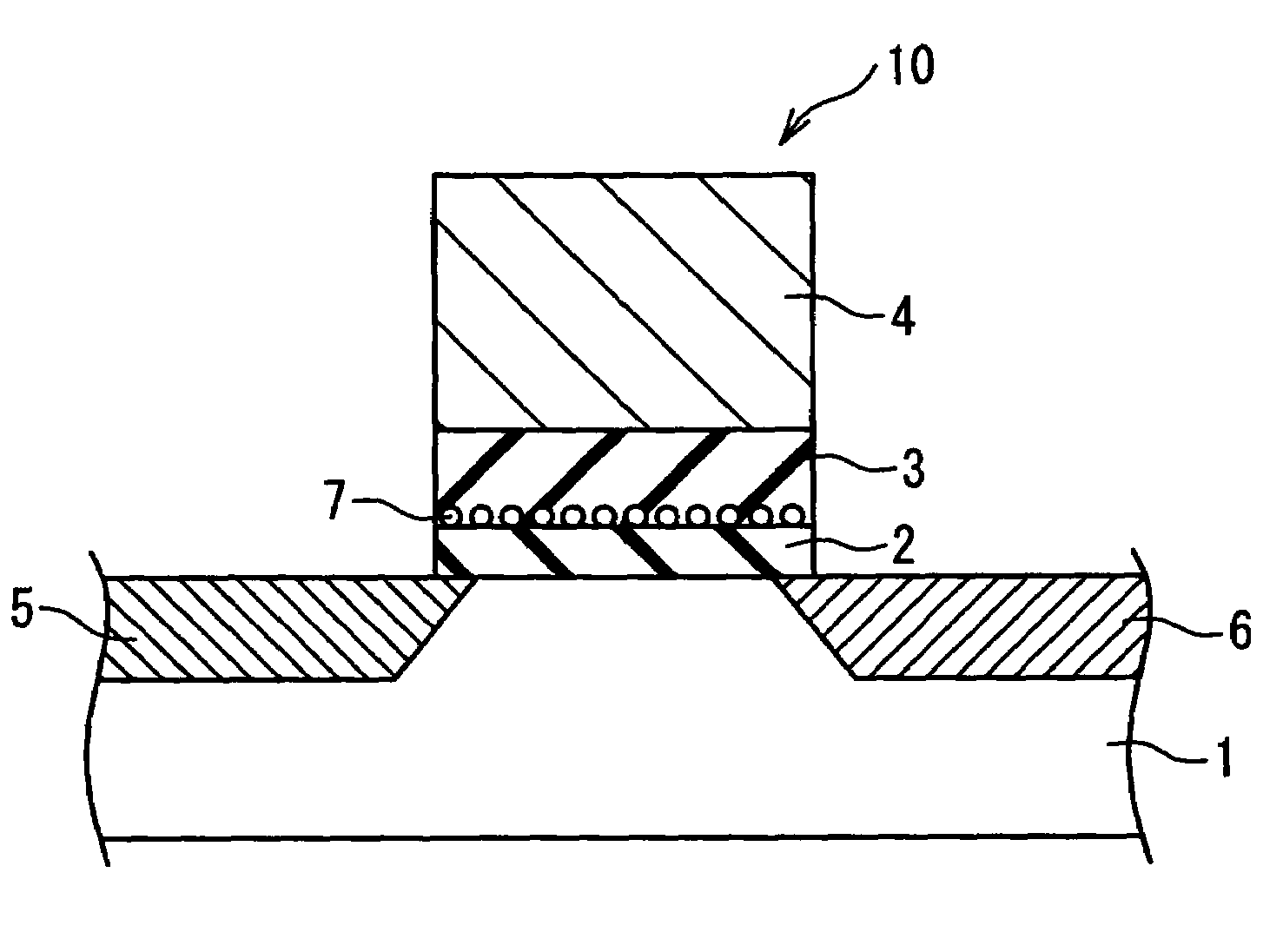
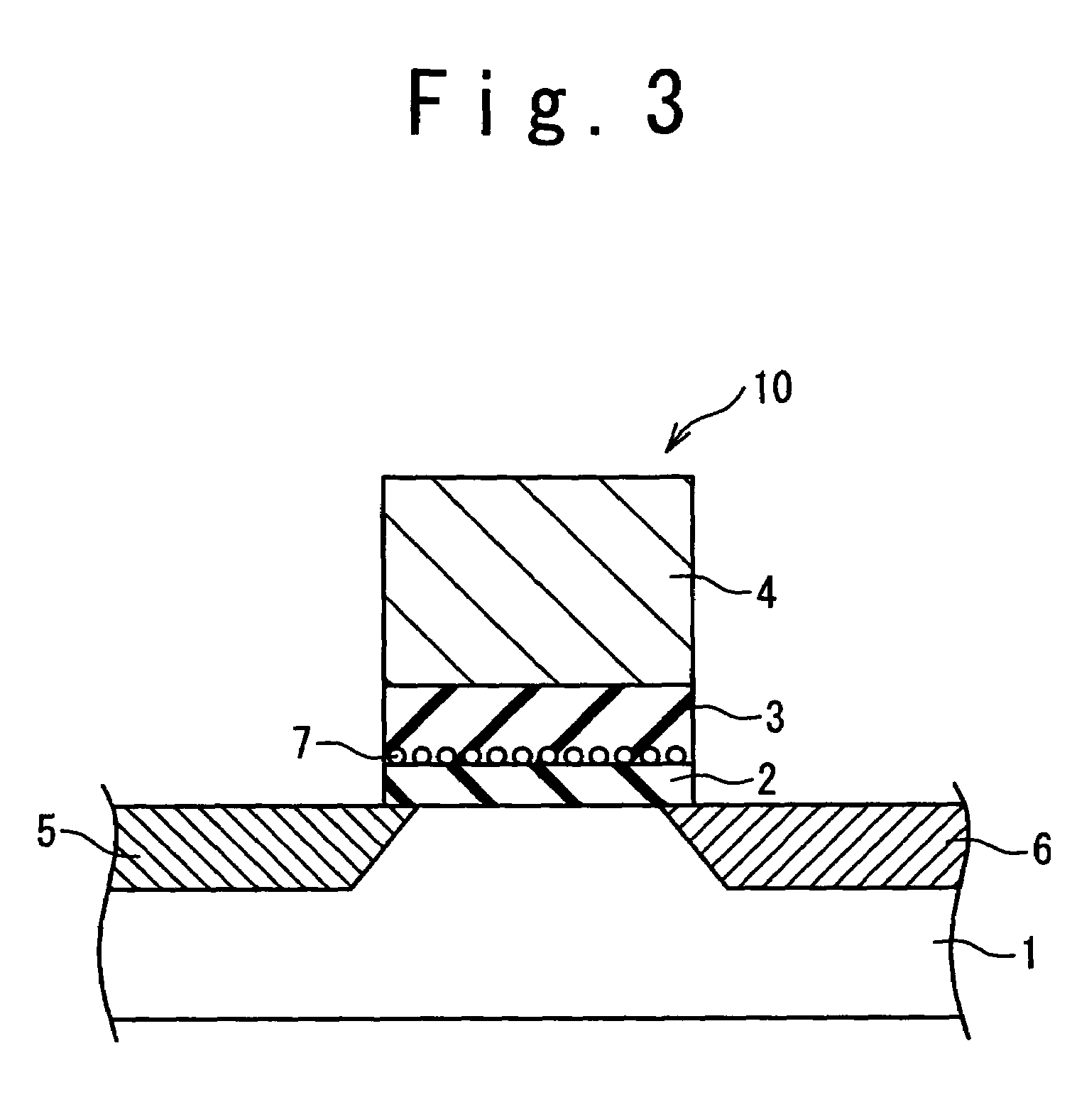
[0076]FIG. 3 is a cross-sectional view showing a cell structure of a non-volatile semiconductor memory device according to the present embodiment. In the non-volatile semiconductor memory device of the present embodiment, a plurality of memory cells are arranged in matrix form. As shown in FIG. 3, in a memory cell 10 of the non-volatile semiconductor memory device according to the present embodiment, a source 5 and a drain 6 are formed in a silicon substrate 1. A channel region is formed between the source 5 and the drain 6. A silicon oxide film 2 having a thickness of 2.0 to 10.0 nm as a first insulating film is formed on the channel region. Also, a plurality of grains 7 (referred to as granular dots, hereinafter) made of silicon are separately formed on the silicon oxide film (first insulating film) 2. The plurality of granular dots 7 serve as a floating gate. A diameter of e...


PUM


Abstract

A non-volatile semiconductor memory device includes a substrate, a first insulating film formed on the substrate, a second insulating film formed on the first insulating film, a plurality of granular dots formed in the second insulating film adjacent to the first insulating film as a floating gate, and a control gate formed on the second insulating film. The second insulating film is a high dielectric constant film made of oxide whose dielectric constant is higher than that of the first insulating film and whose heat of formation is higher than that of silicon oxide.

Description

BACKGROUND OF THE INVENTION[0001]1. Field of the Invention[0002]The present invention relates to a non-volatile semiconductor memory device in which programming and erasing are possible electrically. More particularly, the present invention relates to a non-volatile semiconductor memory device in which a memory cell has a floating gate structure, and a semiconductor device including the non-volatile semiconductor memory device.[0003]2. Description of the Related Art[0004]Conventionally, in a non-volatile semiconductor memory device such as a flash memory and the like, a floating gate made of poly-silicon and the like is formed on a gate oxide film of an n-type MOS transistor. An insulating film such as an ONO (Oxide-Nitride-Oxide) film and the like is formed on the floating gate. A control gate is formed on the insulating film. Each memory cell has such a structure, and a plurality of memory cells are arranged in matrix form. According to the non-volatile semiconductor memory device...

Claims


Application Information

Patent Timeline
Patent Type & Authority Patents(United States)
IPC IPC(8): H01L29/792H01L21/8247H01L27/105H01L27/115H01L29/423H01L29/788
CPCH01L27/105H01L27/11526H01L29/7885H01L29/42332H01L27/11546H10B41/49H10B41/40
Inventor NAKAGAWA, KENICHIROHAMAJIMA, TOMOHIROANDO, KOICHI
Owner RENESAS ELECTRONICS CORP
Why Eureka
Try Eureka