Capacitive temperature, humidity and air pressure sensor integrated manufacturing method based on SOI chip device layer silicon anodic bonding

An air pressure sensor and humidity sensor technology, which is applied in the integrated manufacturing of humidity and air pressure sensors, and capacitive temperature fields, can solve the problems of increased research and development costs, increased research and development difficulty, and long interconnection lines, and achieves improved system reliability and interconnection lines. The effect of length reduction and area reduction

Inactive Publication Date: 2013-12-11
SOUTHEAST UNIV
View PDF8 Cites 16 Cited by
  • Summary
  • Abstract
  • Description
  • Claims
  • Application Information

AI Technical Summary

Problems solved by technology

The advantage of multi-chip assembly technology is that the complexity of a single chip is reduced, so its research and development costs are reduced. The performance of the sensor integrated system is difficult to break through
The second type is to directly integrate multiple sensors on a wafer. This method can overcome many shortcomings of multi-chip assembly technology. Its advantages include system size reduction, interconnection length reduction, reliability improvement, and mass production cost reduction. etc., and its disadvantage will be that the difficulty of research and development will increase, so the cost of research and development will increase

Method used


Image

  • Capacitive temperature, humidity and air pressure sensor integrated manufacturing method based on SOI chip device layer silicon anodic bonding
  • Capacitive temperature, humidity and air pressure sensor integrated manufacturing method based on SOI chip device layer silicon anodic bonding
  • Capacitive temperature, humidity and air pressure sensor integrated manufacturing method based on SOI chip device layer silicon anodic bonding

Examples


Embodiment Construction

[0020] The present invention will be further explained below in conjunction with the accompanying drawings.

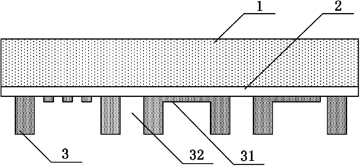
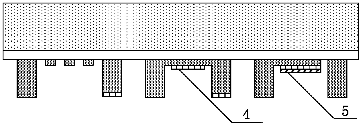
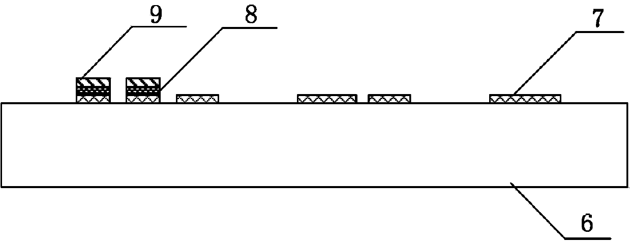
[0021] An integrated manufacturing method for capacitive temperature, humidity and air pressure sensors based on silicon anodic bonding of SOI device layers. The method is realized based on SOI device layer silicon and glass substrate 6. The set substrate silicon 1, the buried oxide layer 2, and the device layer silicon 3 are composed. Using the combination of step-by-step deep silicon etching technology and SOI device layer silicon and glass anode bonding technology, the thin film structure, the flat large capacitance structure and the sealed cavity structure of the air pressure sensor and temperature sensor are prepared at the same time, and finally the humidity sensor and air pressure sensor are formed. Sensor and temperature sensor integrated structure. The method comprises the steps of:

[0022] Step 1), such as figure 1 As shown, the device layer silicon 3 is ...


PUM


Abstract

The invention discloses a capacitive temperature, humidity and air pressure sensor integrated manufacturing method based on SOI chip device layer silicon anodic bonding. According to the integrated manufacturing method, a step-by-step deep silicon etching technology, SOI chip device layer silicon and a glass anodic bonding technology are combined for use so that a thin film structure, a flat large capacitance structure with a tiny electrode gap and a sealed cavity structure needed by an integrated sensor can be manufactured at the same time. The capacitive temperature, humidity and air pressure sensor integrated manufacturing method is characterized in that plenary capacitance sensitive temperature, humidity and air pressure sensors are manufactured in an integrated mode, namely a low power consumption integrated multi-sensor structure is manufactured. The capacitive temperature, humidity and air pressure sensor integrated manufacturing method can be used for realizing on-chip integration of the temperature, humidity and air pressure sensors, therefore, the area of the sensor integrated structure is greatly reduced, the length of an interconnection line is reduced, and the system reliability is improved.

Description

technical field [0001] The invention relates to a manufacturing method of a sensor, in particular to an integrated manufacturing method of a capacitive temperature, humidity and air pressure sensor based on silicon anode bonding of an SOI sheet device layer. Background technique [0002] With the advancement of micromachining technology and the application requirements of miniature intelligent sensor systems, the integration of multiple sensors on a single chip will become a development trend. The on-chip integration methods of multiple sensors can be divided into two categories. The first category is that multiple sensors are manufactured separately and then integrated on the same substrate using multi-chip assembly technology. This type of technology is relatively mature and has been widely used. The advantage of multi-chip assembly technology is that the complexity of a single chip is reduced, so its research and development costs are reduced. The performance of the sens...

Claims


Application Information

Patent Timeline
Patent Type & Authority Applications(China)
IPC IPC(8): G01D21/02
Inventor 王立峰任青颖唐丹黄庆安
Owner SOUTHEAST UNIV
Why Eureka
Try Eureka