

Preparation method of low leakage current HfO2 film suitable for gate dielectric layer
A technology of gate dielectric layer and leakage current, which is applied in coating, metal material coating process, ion implantation plating, etc. Effect
- Summary
- Abstract
- Description
- Claims
- Application Information
AI Technical Summary
Problems solved by technology
Method used
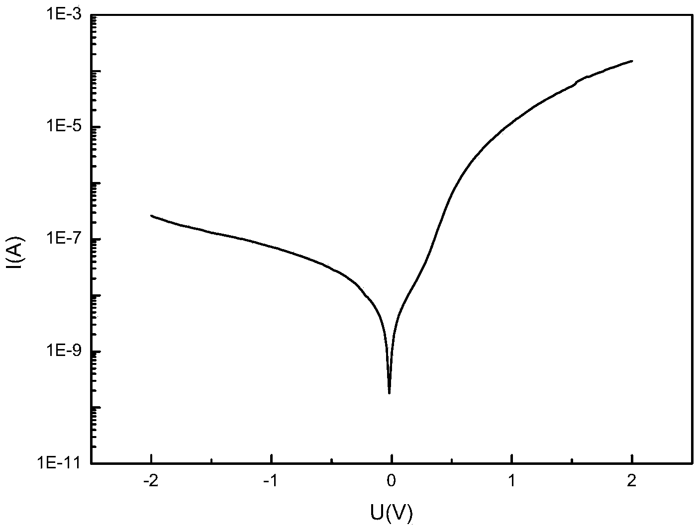
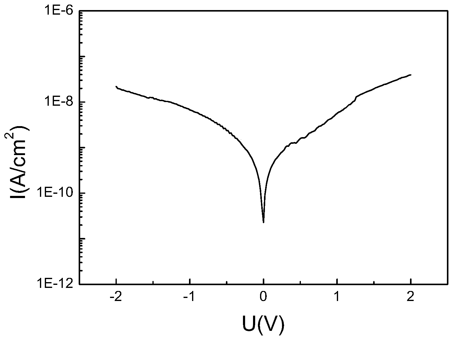
Image

Examples
Embodiment
[0026] In this example, QX-500 high-vacuum multifunctional coating equipment is used. In this example, it is suitable for the low leakage current HfO of the gate dielectric layer. 2 The preparation method of thin film, comprises the steps:
[0027] A. Clean the surface of the silicon substrate, remove the natural oxide layer on the surface of the silicon substrate, and put it into the base of the vacuum chamber.
[0028] In this step, the silicon substrate is an n-type silicon substrate with a resistivity of 10 mm × 10 mm and a crystal orientation (100) of 3-5 Ω·cm. Clean the surface for a fixed period of time to carry out surface cleaning treatment. The fixed period of time is 10 to 15 minutes. After drying, put it into a certain concentration of hydrofluoric acid solution and soak for a period of time to remove the natural oxide layer on the surface of the silicon substrate. The certain concentration may be about 5%, and the period of time is 1 to 2 minutes. The silicon sub...
PUM
 Abstract
Description
Claims
Application Information