High-gain boost converter based on coupling inductance and voltage transfer technology

A boost converter, coupled inductor technology, applied in the direction of output power conversion devices, conversion equipment without intermediate conversion to AC, electrical components, etc., can solve the problem of limited voltage gain, large input current ripple, and switch tube current peaks Large impact and other problems, to improve the power level, reduce switching loss, reduce the effect of current stress

Inactive Publication Date: 2013-12-18
SOUTH CHINA UNIV OF TECH +1
View PDF4 Cites 13 Cited by
  • Summary
  • Abstract
  • Description
  • Claims
  • Application Information

AI Technical Summary

Problems solved by technology

[0003] At present, the most commonly used boost converter is a single-tube Boost converter. However, the boost range of this converter is very limited. Usually, the boost multiple is within ten times, and it is difficult to meet the high-gain conversion requirements.
Although the single-transistor high-gain converter realized by using coupled inductor technology can increase the gain of the converter, the input current ripple is relatively large
Using interleaved parallel technology can reduce the input current ripple but can not achieve the expansion of the converter gain
In order to achieve gain expansion, switched capacitor technology can also be used. This technology has a simple circuit structure and is easy to implement, but it has the disadvantages of large switch current peak impact and limited voltage gain.
Although the voltage gain of the converter can be further expanded through the multi-stage switched capacitor structure, the circuit structure will become very complicated

Method used


Image

  • High-gain boost converter based on coupling inductance and voltage transfer technology
  • High-gain boost converter based on coupling inductance and voltage transfer technology
  • High-gain boost converter based on coupling inductance and voltage transfer technology

Examples


Embodiment 1

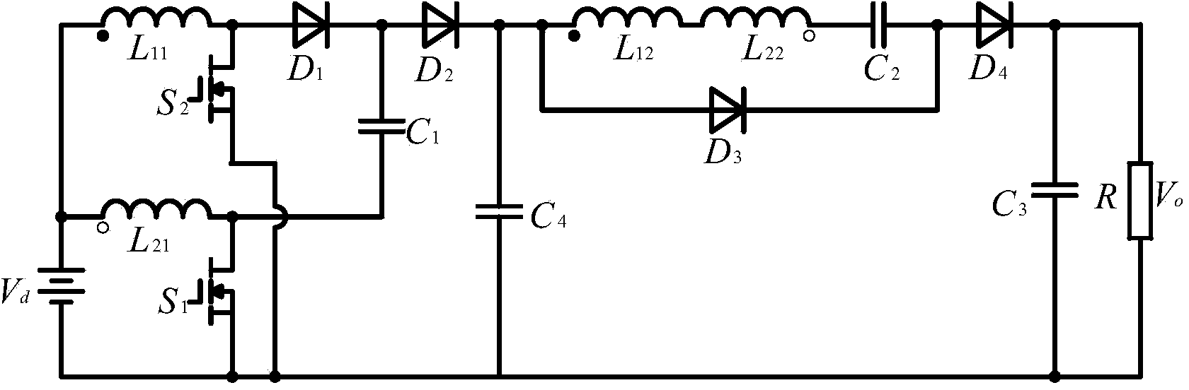
[0029] Such as figure 1 As shown, a high-gain boost converter based on coupled inductors and voltage transfer technology, including sequentially connected asymmetric interleaved parallel Boost circuit, voltage transfer unit circuit, voltage doubler unit circuit and output unit circuit;

[0030] The asymmetric interleaved parallel Boost circuit includes a first switching tube S 1 , the second switch tube S 2 , the first diode D 1 , The primary winding L of the first coupled inductor 11 , The primary winding L of the second coupled inductor 21 ;

[0031] The voltage transfer unit circuit includes a first capacitor C 1 , the fourth capacitor C 4 and the second diode D 2 ;

[0032] The voltage doubler unit circuit includes a secondary winding L of the first coupled inductor 12 , The secondary winding L of the second coupled inductor 22 , the second capacitance C 2 , the third diode D 3 ;

[0033] The output unit circuit includes a fourth diode D 4 , the third capacit...

Embodiment 2

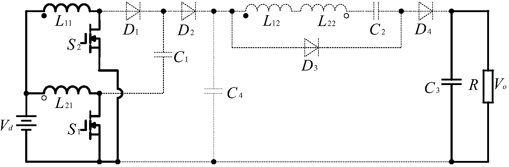
[0073] Such as image 3 , the only difference between this embodiment and embodiment 1 is: the fourth capacitor C 4 The other end is connected to the positive pole of the input power supply, and the rest of the structures and functions are the same as in Embodiment 1.

Embodiment 3

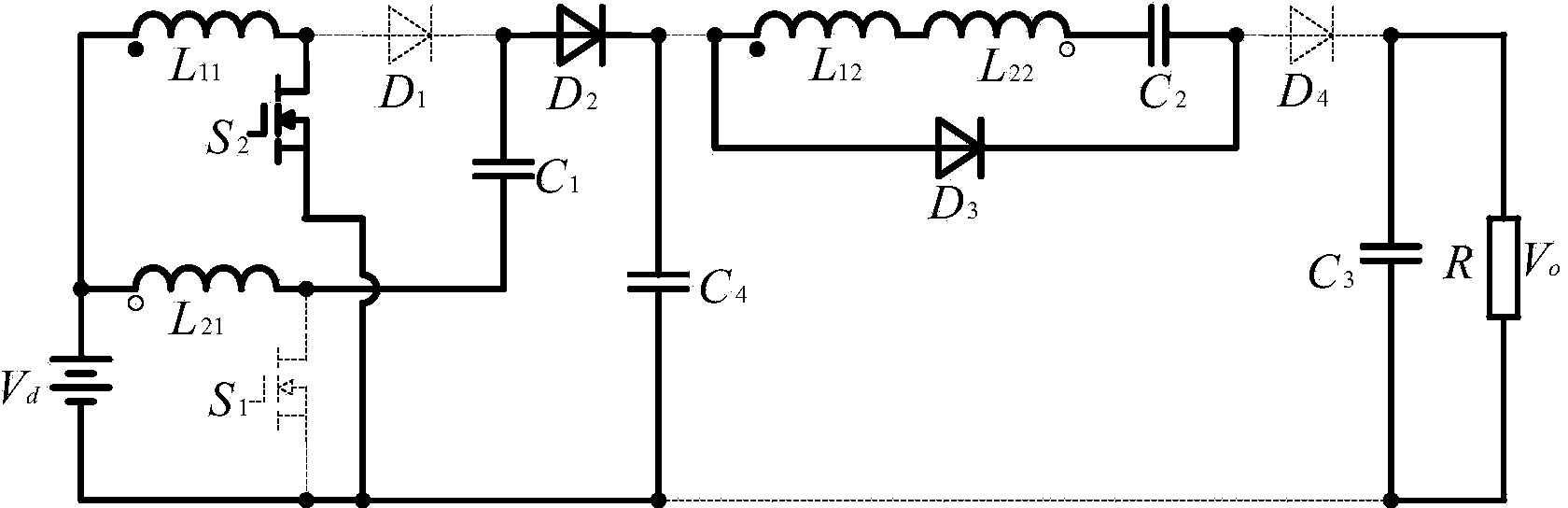
[0075] Such as Figure 4 , the only difference between this embodiment and embodiment 1 is: the fourth capacitor C 4 The other end of the fourth diode D 4 The cathode is connected, and the rest of the structure and function are the same as in Example 1.

[0076] The present invention utilizes a coupled inductor and a second capacitor C 2 The expansion of the voltage gain is realized, and the zero-current turn-on of the switch tube and the zero-current turn-off of the diode are realized by using the leakage inductance of the coupled inductor. 1 , the fourth capacitor C 4 and the second diode D 2 The voltage transfer technology is realized to further increase the voltage gain of the converter, limit the voltage stress borne by the switch tube, and recover leakage inductance energy, and use the asymmetric Boost circuit to reduce the ripple of the input current and reduce the current stress borne by the switch tube .


PUM


Abstract

The invention discloses a high-gain boost converter based on a coupling inductance and voltage transfer technology. The high-gain boost converter comprises an asymmetric interleaving Boost circuit, a voltage transferring unit circuit, a voltage multiplying unit circuit and an output unit circuit, wherein the asymmetric interleaving Boost circuit, the voltage transferring unit circuit, the voltage multiplying unit circuit and the output unit circuit are sequentially connected with one another. The asymmetric interleaving Boost circuit comprises a first switching tube, a second switching tube, a first diode, a primary winding of a first coupling inductor and a primary winding of a second coupling inductor. The voltage transferring unit circuit comprises a first capacitor, a fourth capacitor and a second diode. The voltage multiplying unit circuit comprises an auxiliary winding of the first coupling inductor, an auxiliary winding of the second coupling inductor, a second capacitor and a third diode. The output unit circuit comprises a fourth diode, a third capacitor and a load. According to the high-gain boost converter based on the coupling inductance and voltage transfer technology, the switching losses produced when the converter works are reduced, and the improvement of the power level of the converter is facilitated.

Description

technical field [0001] The invention relates to the technical field of power electronic converters, in particular to a high-gain boost converter based on coupled inductance and voltage transfer technology. Background technique [0002] In a solar power generation system or a fuel cell system, since a single solar cell or a single fuel cell provides low-voltage direct current, and the voltage required in practical applications is usually high, it requires a high-efficiency, low-input The current ripple, high gain, and stable performance boost converter converts low-voltage DC to high-voltage DC suitable for practical needs. [0003] At present, the most commonly used boost converter is a single-tube Boost converter. However, the boost range of this converter is very limited. Usually, the boost multiple is within ten times, and it is difficult to meet the conversion requirements of high gain. Although the single-transistor high-gain converter realized by coupled inductor tech...

Claims


Application Information

Patent Timeline
Patent Type & Authority Applications(China)
IPC IPC(8): H02M3/07H02M1/14
Inventor 张波张能黄子田丘东元肖文勋
Owner SOUTH CHINA UNIV OF TECH
Why Eureka
Try Eureka