Perovskite-based thin film solar cell and method for preparing same

A thin-film solar cell and perovskite technology, which is applied in the field of solar cells, can solve the problems of restricting the development of perovskite-based thin-film solar cells, increasing the cost of battery raw materials, and increasing the cost of battery production, so as to reduce the cost of battery preparation and reduce the thickness of the film. Easy-to-control, easy-to-make effects

Active Publication Date: 2014-01-01
深圳市华物光能技术有限公司
View PDF4 Cites 54 Cited by
  • Summary
  • Abstract
  • Description
  • Claims
  • Application Information

AI Technical Summary

Problems solved by technology

For perovskite-based thin-film solar cells, the biggest disadvantage is that the counter electrode usually uses noble metal electrodes such as gold and silver, which will not only significantly increase the cost of raw materials for the battery, but also the preparation method of noble metal electrodes adopts vacuum evaporation or magnetron control. Sputtering equipment greatly increases the production cost of batteries, and is limited by vacuum evaporation or magnetron sputtering processes, it is difficult to achieve large-scale production, which greatly limits the development of perovskite-based thin film solar cells

Method used


Image

  • Perovskite-based thin film solar cell and method for preparing same
  • Perovskite-based thin film solar cell and method for preparing same
  • Perovskite-based thin film solar cell and method for preparing same

Examples


Embodiment 1

[0075] Prepare 5 parallel solar cells on a piece of conductive glass, the steps are as follows:

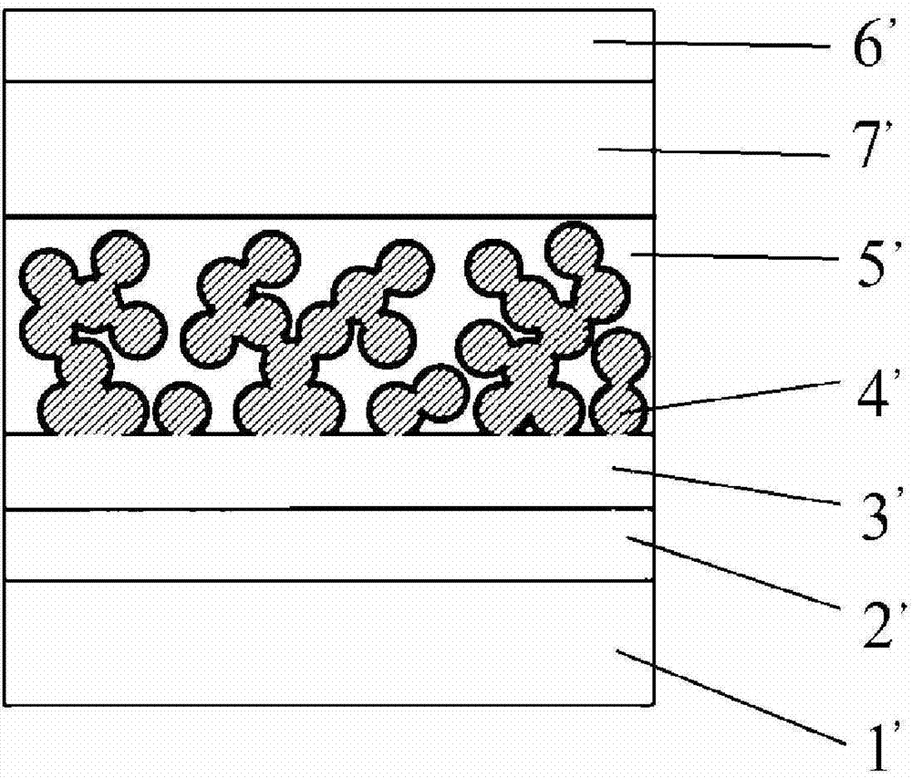
[0076] Conductive glass etching step: cut conductive glass with a size of 20mm (a) × 60mm (b), use a laser cutting machine to etch 4 parallel insulating strips along the direction of the conductive layer b of the conductive glass to divide the conductive glass into 5 sub-areas (each 20mm×12mm). These 5 sub-regions are used to prepare a single solar cell respectively, and the cross-sectional view of each solar cell finally formed is as follows Figure 5 shown. Then on the conductive glass (see Figure 5 ,exist Figure 5 The conductive layer of the middle conductive glass is formed by a transparent substrate 1 and a transparent conductive layer 2) (see Figure 5 On the transparent conductive layer 2), an insulating strip parallel to this side is etched 6mm away from the edge of side b (see Figure 5 Insulating tape 12), divide the conductive glass into the positive electrode ar...

Embodiment 2

[0084] Prepare 5 parallel solar cells on a piece of conductive glass, the steps are as follows:

[0085] Conductive glass etching steps are the same as in Example 1.

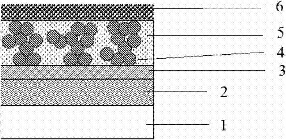
[0086] Screen printing film making steps: use a screen printing machine to print a layer of TiO with a size of 8mm×60mm on the negative electrode area of ​​the cleaned conductive glass 2 The dense layer slurry was dried at 80°C and sintered at 450°C for 30 minutes to obtain dense TiO 2 Thin film, the thickness of the film can be selected between 20-150nm; and then print a layer of ZrO with a size of 8mm×60mm on its surface 2 Nanoparticle slurry, after drying at 80°C and sintering at 500°C for 30 minutes, ZrO 2 Porous film, film thickness can be selected between 200-1500nm; in ZrO 2 Print 5 pieces of carbon paste with a size of 6mm×10mm on the porous film, the 5 pieces of carbon paste are respectively located in a sub-region of the conductive glass, and most of the carbon paste covers the prepared ZrO 2 The o...

Embodiment 3

[0092] Prepare 5 parallel solar cells on a piece of conductive glass, the steps are as follows:

[0093] Conductive glass etching steps are the same as in Example 1.

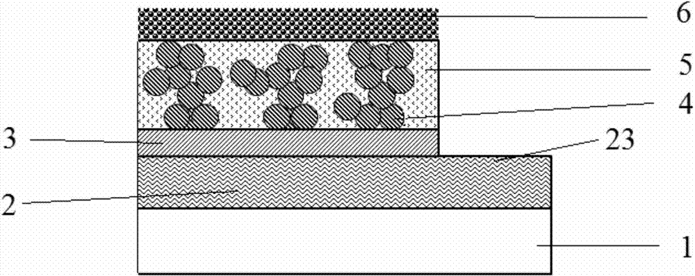
[0094] Screen printing film making steps: use a screen printing machine to print a layer of TiO with a size of 8mm×60mm on the negative electrode area of ​​the cleaned conductive glass 2 The dense layer slurry was dried at 80°C and sintered at 450°C for 30 minutes to obtain dense TiO 2 Thin film, the film thickness can be selected between 20-150nm; then print a layer of SiO with a size of 8mm×60mm on its surface 2 Nanoparticle slurry, dried at 80°C and sintered at 550°C for 30 minutes to obtain SiO 2 Porous film, film thickness can be selected between 200-1500nm; in SiO 2 Print 5 carbon pastes with a size of 6mm×10mm on the porous film, the 5 carbon pastes are respectively located in a sub-region of the conductive glass, and most of the carbon pastes cover the prepared SiO 2 The other part covers the positiv...


PUM

PropertyMeasurementUnit
thicknessaaaaaaaaaa
thicknessaaaaaaaaaa
thicknessaaaaaaaaaa

Abstract

The invention provides a perovskite-based thin film solar cell and a method for preparing the perovskite-based thin film solar cell. The perovskite-based thin film solar cell comprises a transparent substrate, a transparent conducting layer formed on the transparent substrate, a compact layer which is formed on the transparent conducting layer and made of semiconductor materials, a porous insulating layer formed on the compact layer, a porous carbon counter electrode layer formed on the porous insulating layer, and an organic metal semiconductor light absorption material which is filled into pores inside the porous insulating layer and has a perovskite structure. The invention provides application of carbon counter electrodes in the perovskite-based thin film solar cell. Compared with an existing method for preparing the perovskite-based thin film solar cell, the method has the advantages that the counter electrodes are made of carbon materials instead of expensive precious metal materials, and therefore the cost is greatly reduced. The vacuum coating method is replaced by a simple and rapid silk screen print method which allows large-scale production to be achieved, therefore, the cost is further saved, and the achievement of industrial production of the perovskite-based thin film solar cell is facilitated.

Description

technical field [0001] The invention relates to the technical field of solar cells, in particular to a perovskite-based thin film solar cell and a preparation method thereof. Background technique [0002] Solar cells use the photovoltaic effect of specific semiconductor materials to generate electricity. Specifically, the interaction between light and semiconductors generates photogenerated carriers, and photogenerated electron-hole pairs reach the two poles through the built-in electric field formed inside the semiconductor to generate electric potential. When it is connected to an external circuit, it can continuously generate current from a source. This semiconductor optoelectronic device should meet the following two conditions: (1) The energy of the incident light should be greater than the semiconductor band gap, and the semiconductor material has a large enough absorption coefficient for the incident light; (2) The semiconductor has a photovoltaic structure and must b...

Claims


Application Information

Patent Timeline
Patent Type & Authority Applications(China)
IPC IPC(8): H01L51/44H01L51/46H01L51/48
CPCY02E10/549H10K30/82H10K71/00Y02P70/50
Inventor 孟庆波石将建李冬梅罗艳红
Owner 深圳市华物光能技术有限公司
Why Eureka
Try Eureka