A kind of carbon electrode material of perovskite thin film solar cell and preparation method thereof
A solar cell and perovskite technology, applied in the direction of photosensitive equipment, etc., can solve the problems of large-scale promotion of unsuitable technology, high requirements for experimental conditions, and high cost, and achieve the effects of easy control of film thickness, cost reduction, and low cost
- Summary
- Abstract
- Description
- Claims
- Application Information
AI Technical Summary
Problems solved by technology
Method used
Image
Examples
Embodiment 1
[0022] (1) Preparation of dense titanium dioxide film layer
[0023] Put diisopropyl di(acetylacetonate) titanate (TiAcAc) into a beaker, add C2H5OH, the molar ratio of raw materials is TiAcAc:C 2 h 5 OH=1:30, stirred for 0.5 hours, the above solution was sprayed to form a film on the transparent conductive FTO substrate, and the sprayed sample was sintered at 500 ° C for 0.5 hours to prepare a dense titanium dioxide film layer.
[0024] (2) Preparation and assembly process of solar cells
[0025] Preparation of the light-absorbing layer of the perovskite film: under an inert atmosphere, spin-coat PbI on the above-mentioned dense titanium dioxide film layer by liquid phase method 2 solution, heated at 110°C for 5 minutes; impregnated with prepared CH 3 NH 3 I solution, reacted for 30 minutes, took it out and washed it in IPA solution; finally put it in an environment of 70 ° C for 30 minutes to dry.
[0026] (3) Preparation of hole transport layer / carbon thin film layer ...
Embodiment 2
[0029] (1) Preparation of dense titanium dioxide film layer
[0030] Refer to the preparation process of the dense titanium dioxide thin film layer in Example 1.
[0031] (2) Preparation and assembly process of solar cells
[0032] Refer to the preparation and assembly process of the solar cell in Example 1.
[0033] (3) Preparation of carbon counter electrode:
[0034] Referring to the preparation process of the carbon counter electrode in Example 1, the spraying time was adjusted to 150s.
Embodiment 3
[0036] (1) Preparation of dense titanium dioxide film layer
[0037] Refer to the preparation process of the dense titanium dioxide thin film layer in Example 1.
[0038] (2) Preparation and assembly process of solar cells
[0039] Refer to the preparation and assembly process of the solar cell in Example 1.
[0040] (3) Preparation of hole transport layer / carbon electrode
[0041] Referring to the preparation process of the carbon counter electrode in Example 1, the spraying time was adjusted to 50s.
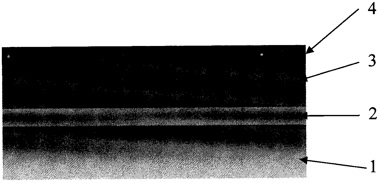
[0042] combined with figure 1 Schematic representation of the structure of a perovskite thin film solar cell, where the hole transport layer / carbon thin film layer is figure 1 Schematic diagram of the thin film referred to in middle 4, that is, the carbon electrode layer of the perovskite thin film solar cell.
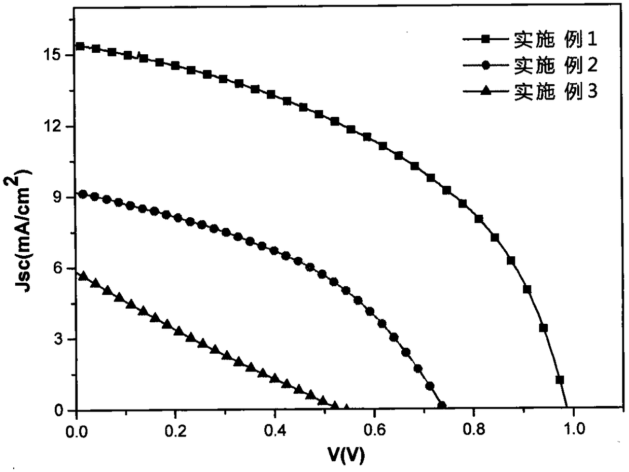
[0043] combine figure 2 with image 3It can be further illustrated that the operation of the present invention is highly controllable. The resistance of the h...
PUM
| Property | Measurement | Unit |
|---|---|---|
| thickness | aaaaa | aaaaa |
Abstract
Description
Claims
Application Information


