Light guide plate, planar light emitting device, liquid crystal display device, liquid crystal display terminal equipment and manufacturing method of light guide plate

A technology of light guide plate and light plane, applied in the field of light guide plate, can solve the problems of large loss of light energy, inability to transmit light, destroy the principle of total reflection of light guide plate, etc., and achieve the effect of good light efficiency effect.

Inactive Publication Date: 2014-01-08
HANGZHOU RUIHUI OPTOELECTRONICS TECH
View PDF14 Cites 12 Cited by
  • Summary
  • Abstract
  • Description
  • Claims
  • Application Information

AI Technical Summary

Problems solved by technology

There is also the patent announcement of patent No. 02152108.5, which is to add 10 um-50 um organic filler spheres into the adhesive and evenly coat the light-emitting plane of the light guide plate. The water agent used here is generally similar to chloroform. Acrylic adhesive instead of paste adhesive, and the entire surface is coated instead of patterned, which destroys the principle of total reflection of the light guide plate, so that the light cannot be transmitted to the central area, and their The purpose of the invention is to replace the role of the diffusion film to save the cost of the backlight module
The screen printing light guide plate of the prior art not only loses a lot of light energy in the process of light transmission and conversion, but also releases toxic gas during the production process to damage the health of production employees, so it has long been eliminated in the field of small size, but production The small-sized injection molding production process cannot be realized on the large-sized light guide plate

Method used


Image

  • Light guide plate, planar light emitting device, liquid crystal display device, liquid crystal display terminal equipment and manufacturing method of light guide plate
  • Light guide plate, planar light emitting device, liquid crystal display device, liquid crystal display terminal equipment and manufacturing method of light guide plate
  • Light guide plate, planar light emitting device, liquid crystal display device, liquid crystal display terminal equipment and manufacturing method of light guide plate

Examples


Embodiment 1

[0086] Example 1: Reference Figure 22 , 5 , 12, 14, 15, 16, 20, 1, 9, 10, 21, 27, 32-inch LCD TV light guide plate and its LCD TV

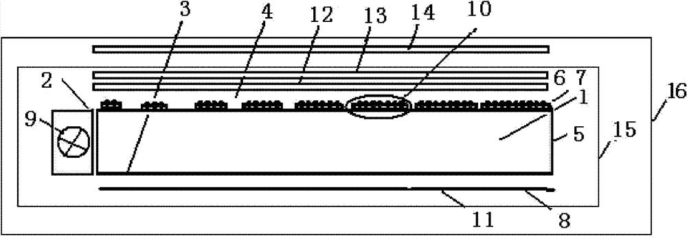
[0087] Picture 10 It is a schematic diagram of the side structure of a 32-inch LCD TV honeycomb-shaped high-efficiency and energy-saving microstructure light guide plate. The light guide plate includes a colorless and transparent methyl methacrylate flat-plate substrate 1. A light-incident side end surface for receiving light into the interior 2 , The light-emitting plane 4 that is opposite to the light-incident side end face and intersects with the reflective side end face 5 coated with a reflective film, and the light that intersects the light exiting plane 4 from the inside, and the bottom plane 3 with the scattering microstructure pattern opposite to the light-emitting plane 4 Structure, wherein the microstructure scattering three-dimensional pattern layer on the bottom plane 3 is formed by coating the bottom plane of the substrate with a layer ...

Embodiment 2

[0096] Example 2, reference Figure 23 , 11 , 12, 17, 18, 19, 20, 3, 21, 27, 42-inch light guide plate and its LCD TV

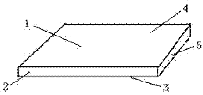
[0097] Picture 11 It is a schematic diagram of the side structure of the honeycomb-shaped high-efficiency energy-saving microstructure light guide plate of a 42-inch LCD TV, including a colorless and transparent methyl methacrylate flat plate substrate 1, at least one light-incident side end surface for receiving light into the interior 2, The light exit plane 4 opposite to the light entrance side end surface and the other intersecting reflective side end surface 5 coated with a reflective film, and the light that intersects the light exiting from the inside, and a bottom plane 3 with a scattering microstructure pattern opposite to the light exit plane 4 , Wherein the microstructure scattering pattern on the bottom plane 3 is formed by coating the bottom plane of the substrate with a layer such as Figure 5 The distribution pattern shown is used to adjust the ov...

Embodiment 3

[0105] Example 3: Reference Figure 24 , 2 , 13, 14, 15, 16, 20, 21, 27, 14 inch light guide plate and its laptop

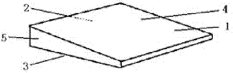
[0106] Figure 24 It is a 14-inch colorless and transparent PC wedge substrate 1 (such as figure 2 ) Is a schematic diagram of the side structure of a honeycomb-shaped high-efficiency energy-saving microstructure light guide plate for a laptop computer, the light guide plate includes a colorless and transparent wedge-shaped PC substrate 1, at least one light-incident side end surface 2 for receiving light into the interior, and a light-incident side end surface The remaining opposite and intersecting reflective side end faces 5 are pasted with reflective films, and the light exiting plane 4 from which the intersecting light exits from the inside and the bottom plane 3 opposite to the light exiting plane 4 with a scattering microstructure pattern are formed, wherein the bottom plane 3 The micro-structure scattering three-dimensional pattern layer on the substrate is ...


PUM

PropertyMeasurementUnit
particle diameteraaaaaaaaaa
thicknessaaaaaaaaaa
particle diameteraaaaaaaaaa

Abstract

The invention discloses an efficient energy-saving microstructural light guide plate, a planar light emitting device provided with the light guide plate, a liquid crystal display device, liquid crystal display terminal equipment and a manufacturing method of the light guide plate. A scattering pattern structure on the bottom plane of the light guide plate is formed by providing a colorless and transparent adhesive glue pattern layer on the bottom plane of the substrate, a stereoscopic microstructural scattering pattern layer is obtained by planting and sticking a plurality of mini scattering particles on the adhesive glue pattern layer, all or part of the planted and stuck mini scattering particles is bared and protrudes at the surface of the adhesive glue pattern layer, a part of the mini scattering particles, which is bared and protrudes at the surface of the adhesive glue pattern layer, is embedded into the colorless and transparent adhesive glue pattern layer, and is firmly bonded by the adhesive glue, and the other part of the mini scattering particles is bared and protrudes outside the colorless and transparent adhesive glue pattern layer. After adopting the light guide plate, a brightness increase rate of the planar light emitting device is more than 20%. According to the light guide plate prepared by the invention, the light guide plates in small, middle and big sizes can be manufactured at high quality, and the brightness increase rate of the light guide plate is fully realized.

Description

Technical field [0001] The invention relates to a light guide plate, a planar light emitting device, a liquid crystal display device, and a liquid crystal display terminal device. The invention also relates to a method of manufacturing the light guide plate. Background technique [0002] Generally, a liquid crystal display device includes a liquid crystal display panel that displays images and a flat light emitting device that supplies light to the liquid crystal display panel. The liquid crystal display panel includes two transparent substrates and a liquid crystal layer disposed between the two substrates to display images in response to changes in the arrangement of liquid crystal molecules of the liquid crystal layer caused by electrical signals. [0003] Planar light-emitting devices are classified into direct-lit planar light-emitting devices and edge-lit planar light-emitting devices according to the location of the light source. [0004] The direct type planar light emitting...

Claims


Application Information

Patent Timeline
Patent Type & Authority Applications(China)
IPC IPC(8): G02B6/00G02F1/13357F21S8/00F21V8/00F21Y101/02
CPCG02B6/0043G02B6/006G02B6/0061
Inventor 唐龙
Owner HANGZHOU RUIHUI OPTOELECTRONICS TECH
Why Eureka
Try Eureka