GaN-based light-emitting diode epitaxial wafer and manufacturing method thereof

A technology of light-emitting diodes and epitaxial wafers, applied in electrical components, circuits, semiconductor devices, etc., can solve the problems of limited carrier binding capacity, low internal quantum efficiency, lattice mismatch, etc. , The effect of high internal quantum efficiency and low stress

Active Publication Date: 2014-01-08
HC SEMITEK CORP
View PDF7 Cites 26 Cited by
  • Summary
  • Abstract
  • Description
  • Claims
  • Application Information

AI Technical Summary

Problems solved by technology

[0005] InGaN quantum well layer and GaN quantum barrier layer will produce lattice mismatch due to different materials, resulting in stress in the multi-quantum well layer, which will cause piezoelectric polarization effect, and form a piezoelectric polarization field in the multi-quantum well layer. The energy bands of the InGaN quantum well layer and the GaN quantum ba

Method used


Image

  • GaN-based light-emitting diode epitaxial wafer and manufacturing method thereof
  • GaN-based light-emitting diode epitaxial wafer and manufacturing method thereof
  • GaN-based light-emitting diode epitaxial wafer and manufacturing method thereof

Examples


Embodiment 1

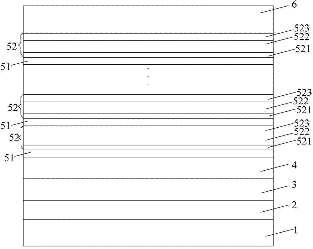
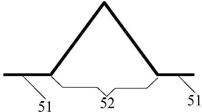
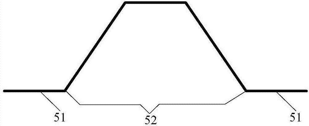
[0037] The embodiment of the present invention provides a GaN light emitting diode epitaxial wafer, see figure 1 , The epitaxial wafer includes: a substrate 1 and a buffer layer 2, an undoped GaN layer 3, an n-type layer 4, a multiple quantum well layer, and a p-type layer 6, which are sequentially grown on the substrate 1. The multiple quantum well layer is Multi-period structure, each period includes an InGaN quantum well layer 51 and a quantum barrier layer 52 grown on the InGaN quantum well layer 51. The quantum barrier layer 52 includes a first InGaN layer 521 and AlGaN grown sequentially on the first InGaN layer 521 Layer 522 and second InGaN layer 523.

[0038] It should be noted that in the multiple quantum well layer, the In composition content of each quantum barrier layer 52 is less than the In composition content of each InGaN quantum well layer 51 to ensure that the band gap of the quantum barrier layer 52 is greater than that of the InGaN quantum well layer. Band ga...

Embodiment 2

[0055] The embodiment of the present invention provides a method for manufacturing a GaN-based light-emitting diode epitaxial wafer, such as Figure 8 As shown, the method includes:

[0056] Step 501: Provide a substrate;

[0057] Optionally, in this embodiment, the substrate may be a sapphire substrate. Obviously, the substrate may also be a Si substrate, a SiC substrate, or the like.

[0058] Step 502: sequentially growing a buffer layer, an undoped GaN layer, and an n-type layer on the substrate;

[0059] Optionally, in this embodiment, the n-type layer may be an n-type GaN layer, and the n-type GaN layer may be a single layer or multiple layers.

[0060] Step 503: Growing a multiple quantum well layer on the n-type layer, the multiple quantum well layer has a multi-period structure, and each period includes an InGaN quantum well layer and a quantum barrier layer grown on the InGaN quantum well layer;

[0061] The quantum barrier layer of each period of growth, including:

[0062] Gro...


PUM

PropertyMeasurementUnit
Thicknessaaaaaaaaaa
Thicknessaaaaaaaaaa

Abstract

The invention discloses a GaN-based light-emitting diode epitaxial wafer and a manufacturing method of the GaN-based light-emitting diode epitaxial wafer, and belongs to the technical field of semiconductors. The GaN-based light-emitting diode epitaxial wafer comprises a substrate, a buffering layer, an undoped GaN layer, an n-type layer, a multiple-quantum-well layer and a p-type layer, wherein the multiple-quantum-well layer is of a multi-cycle structure, each cycle of the multiple-quantum-well layer comprises an InGaN quantum-well layer and a quantum barrier layer which grows on the InGaN quantum-well layer, each quantum barrier layer comprises a first InGaN layer, an AlGaN layer and a second InGaN layer, and each AlGaN layer and each second InGaN layer grow on each first InGaN layer in sequence. According to the scheme, the first InGaN layer and the second InGaN layer of each quantum barrier layer make contact with each InGaN quantum-well layer, the InGaN quantum-well layers, the first InGaN layers and the second InGaN layers are made of the same materials, the degree of lattice mismatch is low, produced stress is low, the effect of a piezoelectric polarization electric field is poor, the degree of band bending of the InGaN quantum-well layers and the quantum barrier layers becomes lower, the capacity of restraining charge carriers is improved, and when high current is injected, serious leakage current cannot be formed.

Description

Technical field [0001] The present invention relates to the field of semiconductor technology, in particular to a GaN-based light emitting diode epitaxial wafer and a manufacturing method thereof. Background technique [0002] GaN (Gallium Nitride) is a typical representative of the third-generation wide-bandgap semiconductor materials. Its excellent high thermal conductivity, high temperature resistance, acid and alkali resistance, and high hardness make it widely used in blue, green, UV light-emitting diodes. The core component of a GaN-based light-emitting diode is a chip, which includes an epitaxial wafer and electrodes arranged on the epitaxial wafer. [0003] GaN-based light-emitting diode epitaxial wafers generally include a substrate and a buffer layer, an undoped GaN layer, an n-type layer, a multiple quantum well layer, and a p-type layer that are sequentially grown upward on the substrate. The multiple quantum well layer is made of InGaN A multilayer structure formed b...

Claims


Application Information

Patent Timeline
IPC IPC(8): H01L33/06H01L33/28H01L33/00
CPCH01L33/0075H01L33/06H01L33/32
Inventor 吉亚莉魏世祯陈柏松胡加辉谢文明
Owner HC SEMITEK CORP
Why Eureka
Try Eureka