embossing material

A film substrate and compound technology, applied in thin material processing, nanotechnology, coating, etc., can solve the problem of not being able to obtain the target pattern shape, etc., and achieve mold release force suppression, low mold release force, and high stability Effect

Inactive Publication Date: 2016-01-13
NISSAN CHEM CORP
View PDF14 Cites 0 Cited by
  • Summary
  • Abstract
  • Description
  • Claims
  • Application Information

AI Technical Summary

Problems solved by technology

[0006] However, it was pointed out that in optical nanoimprint lithography, the imprint material adheres to the mold as the metal mold after imprinting, and sometimes the target pattern shape cannot be obtained.

Method used


Image

  • embossing material
  • embossing material
  • embossing material

Examples


Embodiment

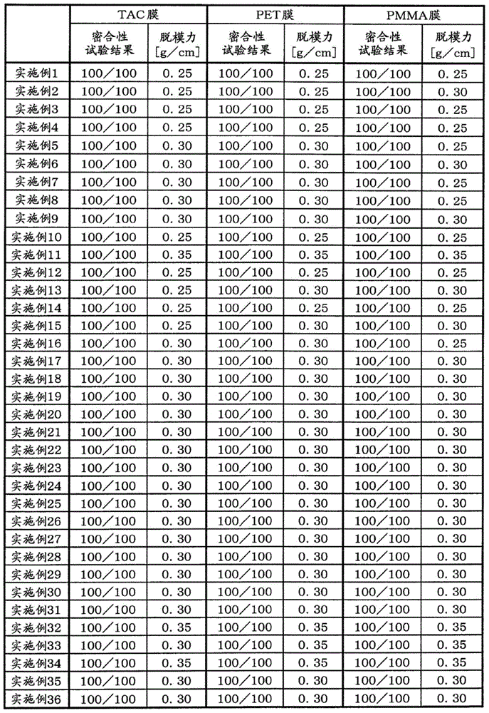
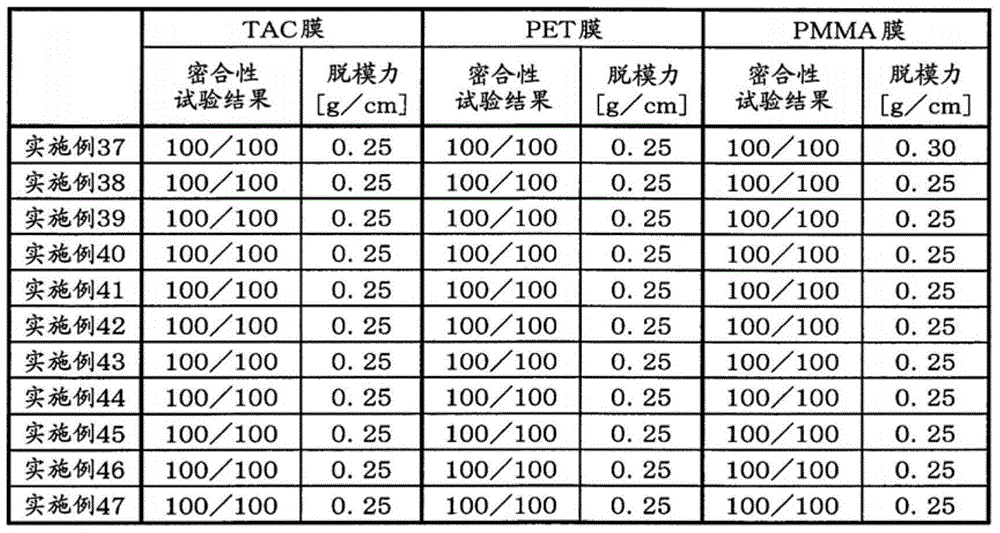
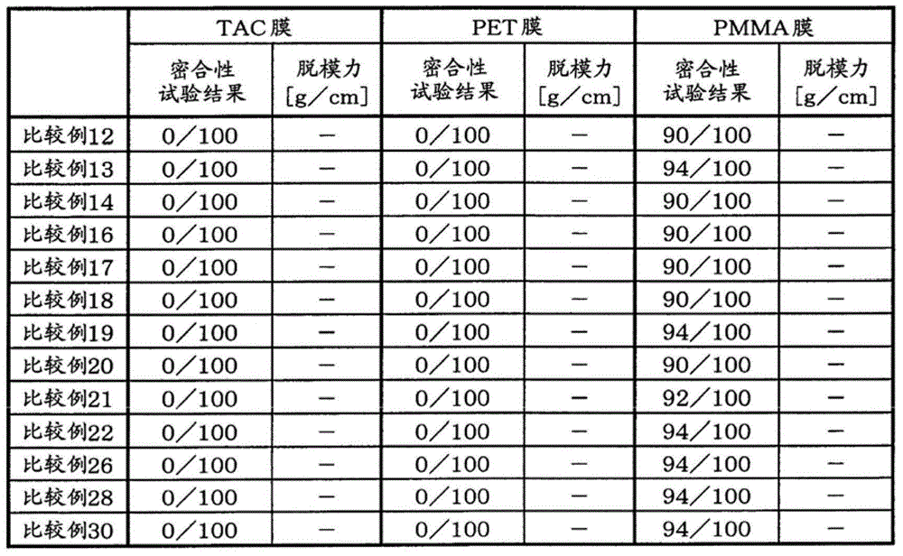
[0131] Hereinafter, although an Example and a comparative example are given and this invention is demonstrated in more detail, this invention is not limited to these Examples.

[0132] In addition, each measuring device used in the examples is as follows.

[0133] [Exposure machine]

[0134] Device: Electrodeless uniform irradiation device QRE-4016A manufactured by Oak Manufacturing Co., Ltd.

[0135] [UV-visible spectrophotometer]

[0136] Device: SHIMADSUUV-3600 manufactured by Shimadzu Corporation

[0137] [Adhesion test]

[0138] Standard: JISK5400

[0139] [Automatic Film Maker]

[0140] Device: KT-AB3120 manufactured by Cortec Co., Ltd.

[0141] [Removal of molds]

[0142] A nickel-made motheye pattern mold with a pitch of 250 nm and a height of 250 nm (manufactured by Inox Co., Ltd.) and a silicon substrate used in the photocurability test described later were immersed in Nobeck (registered trademark) HFE-7100 (hydrogen fluorine Ether, Sumitomo Three-Em Co., Ltd...

Embodiment 2

[0147] Imprint material A2 (solid content: 50% MEK solution) was prepared in the same manner as in Example 1 except that A-200 in Example 1 was changed to A-400 (manufactured by Shin-Nakamura Chemical Industry Co., Ltd.).

Embodiment 3

[0149] Imprint material A3 (solid content: 50% MEK solution) was prepared in the same manner as in Example 1 except that A-200 in Example 1 was changed to A-600 (manufactured by Shin-Nakamura Chemical Industry Co., Ltd.).


PUM

PropertyMeasurementUnit
boiling pointaaaaaaaaaa

Abstract

The subject of the present invention is to provide an imprint of a film that is in the form of a transparent and uniform varnish that does not peel off in a cross-cut test for evaluating the adhesion of a coating film, and that has a release force of 0.5 g / cm or less. Material. Means for solving the problem of the present invention relates to an imprint material comprising: (A) component: a compound having at least one oxyalkylene unit having 2, 3, or 4 carbon atoms and having at least 2 polymerizable groups , (B) component: photopolymerization initiator, (C) component: the solvent which swells or dissolves the surface part of a film base material, and (D) component: organosilicon compound.

Description

technical field [0001] The present invention relates to an imprint material (film-forming composition for imprint) and a film produced from the material and onto which a pattern is transferred. More specifically, it relates to an imprint material whose formed film has high adhesion to a film substrate and low release force, and a film produced from the material and onto which a pattern is transferred. Background technique [0002] In 1995, a new technique called nanoimprint lithography was proposed by Professor Chou, now at Princeton University (Patent Document 1). In nanoimprint lithography, a mold having an arbitrary pattern is brought into contact with a base material on which a resin film is formed, the resin film is pressed, and heat or light is used as an external stimulus to form a target pattern on the cured resin film. This nanoimprint lithography has the advantage of being able to perform nanoscale processing easily and inexpensively compared with conventional pho...

Claims


Application Information

Patent Timeline
Patent Type & Authority Patents(China)
IPC IPC(8): H01L21/027B29C59/02C08F2/44C08F2/50B29K33/00
CPCC08F2/44C08F2/50C08F222/102G03F7/0002G03F7/0048G03F7/027G03F7/0757B82Y10/00B82Y40/00H01L27/14625Y10T428/24479Y10T428/24612Y10T428/24802B29C33/62B29C59/02C08F20/26C08F220/26C08J7/04C08L33/14C08L83/04H01L21/027H01L31/02167B32B3/30C08L33/08
Inventor 加藤拓小林淳平首藤圭介铃木正睦
Owner NISSAN CHEM CORP
Why Eureka
Try Eureka