

Preparation method of copper nanowire arrays with porous structure and film conductivity measuring method thereof
A technology of copper nanowires and arrays, applied in the field of preparing copper nanowire arrays, can solve the problems of poor repeatability of the reaction, restrictions on large-scale production of copper nanowires, slow reaction time, etc.
- Summary
- Abstract
- Description
- Claims
- Application Information
AI Technical Summary
Problems solved by technology
Method used
Image

Examples
Embodiment 1
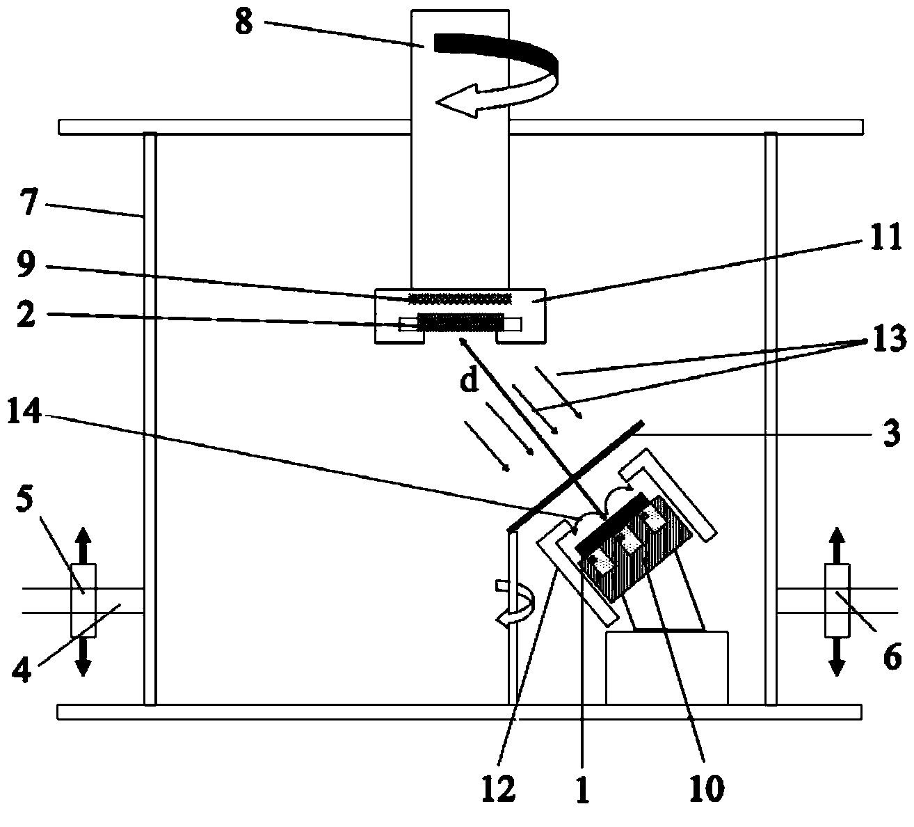
[0039] Magnetron sputtering apparatus: JGP-450a multi-target magnetron sputtering deposition system (Shenyang Scientific Instrument Development Center Co., Ltd., Chinese Academy of Sciences);
[0040] Substrate type: aluminum nitride;
[0041] Adjust the distance d=90mm between the sample stage 2 and the radio frequency stage 1;
[0042] Vacuumize the vacuum chamber 7 to make the vacuum degree in the vacuum chamber 7 reach 3.4×10 -4 Pa;
[0043] Turn on the heating control power supply 9, and turn on the sample rotation stage 8 to keep the substrate temperature at room temperature;
[0044] Fill the vacuum chamber 7 with argon, and adjust the air pressure to 1.5Pa;
[0045] Adjust the DC current to 110mA and the voltage to 0.30kV
[0046] Deposition time 2h;
[0047] After the preparation, turn off the DC power supply, anneal in situ for 20 minutes, and cool naturally to room temperature 25° C., then take out the aluminum nitride substrate with the copper nanowire array t...
Embodiment 2
[0050] Magnetron sputtering apparatus: JGP-450a multi-target magnetron sputtering deposition system (Shenyang Scientific Instrument Development Center Co., Ltd., Chinese Academy of Sciences)
[0051] Adjust the distance d=90mm between sample stage 2 and RF stage 1
[0052] Vacuumize the vacuum chamber 7 to make the vacuum degree in the vacuum chamber 7 reach 3.4×10 -4 Pa;
[0053] Turn on the heating control power supply 9, and turn on the sample rotation table 8, so that the substrate temperature rises to 100°C;
[0054] Rush into the vacuum chamber 7 with argon, and adjust the air pressure to 1.5Pa;
[0055] Adjust the DC current to 110mA and the voltage to 0.30kV
[0056] Deposition time 2h;
[0057] After the preparation, turn off the DC power supply, anneal in situ for 20 minutes, and cool naturally to room temperature 25° C., then take out the aluminum nitride substrate with the copper nanowire array thin film.
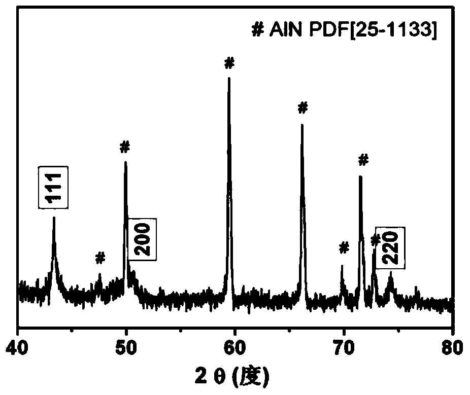
[0058] Adopt X-ray diffractometer to carry out phase ...
Embodiment 3
[0060] Magnetron sputtering apparatus: JGP-450a multi-target magnetron sputtering deposition system (Shenyang Scientific Instrument Development Center Co., Ltd., Chinese Academy of Sciences)
[0061] Substrate type: aluminum nitride;
[0062] Adjust the distance d=90mm between sample stage 2 and RF stage 1
[0063] Vacuumize the vacuum chamber 7 to make the vacuum degree in the vacuum chamber 7 reach 3.4×10 -4 Pa;
[0064] Turn on the heating control power supply 9, and turn on the sample rotation table 8, so that the substrate temperature rises to 200°C;
[0065] Rush into the vacuum chamber 7 with argon, and adjust the air pressure to 1.5Pa;
[0066] Adjust the DC current to 110mA and the voltage to 0.30kV
[0067] Deposition time 2h;
[0068] After the preparation, turn off the DC power supply, anneal in situ for 20 minutes, and cool naturally to room temperature 25° C., then take out the aluminum nitride substrate with the copper nanowire array thin film.
[0069] Ad...
PUM
| Property | Measurement | Unit |
|---|---|---|
| diameter | aaaaa | aaaaa |
| thickness | aaaaa | aaaaa |
| thickness | aaaaa | aaaaa |
Abstract
Description
Claims
Application Information