An In-Situ Plasma Glow Treatment Method for Improving the Field Emission Properties of Tungsten Oxide Nanomaterial Thin Films
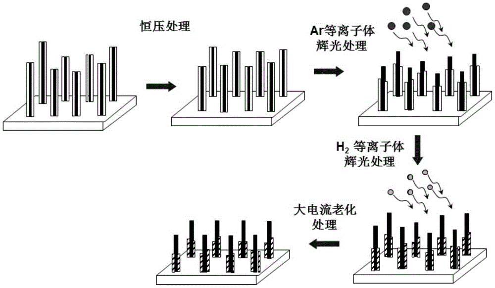
A material thin film and plasma technology, applied in discharge tubes, electrical components, circuits, etc., can solve problems such as differences in structure and physical properties, achieve simple equipment, low method cost, and improve field emission characteristics
- Summary
- Abstract
- Description
- Claims
- Application Information
AI Technical Summary
Problems solved by technology
Method used
Image
Examples
Embodiment 1
[0034] Example 1: In-situ plasma process processing a sample of tungsten oxide nanowire thin film with poor uniformity
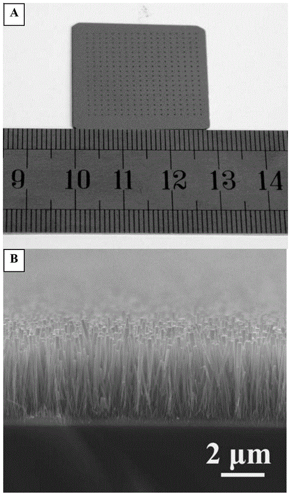
[0035] The sample 1 of the tungsten oxide nanowire thin film with poor emission uniformity prepared by the thermal evaporation growth method was treated with an in-situ plasma process. The total area of the substrate is 2.8×2.8cm 2 , The shape of the nanowire pattern is circular and the diameter is 300μm. Since there are 18 nanowire patterns in each row and column on the substrate, the total number of nanowire patterns on the substrate is 324, and the total emission area is 0.229cm 2 .
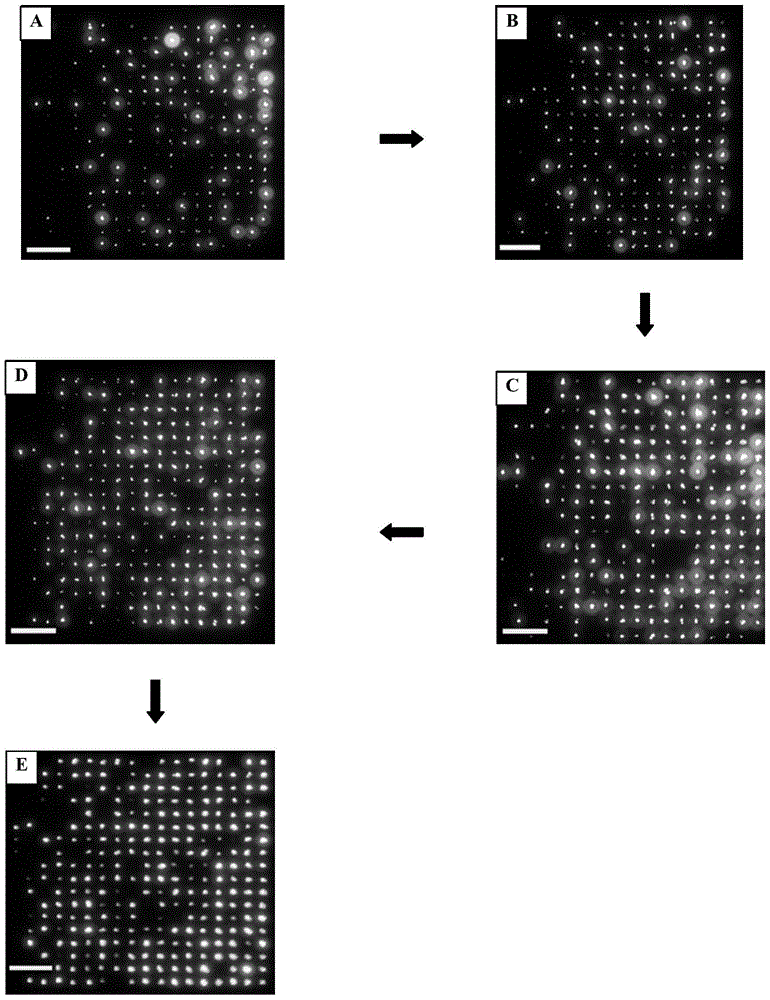
[0036] First, the patterned tungsten oxide nanowire array (sample 1, seen in figure 2 ) As the cathode of the two-pole field emission structure, it is placed in a high vacuum chamber. The anode is a phosphor screen coated with phosphor, the distance between the anode and cathode is 400μm, and the background vacuum of the system is 2.0×10 -5 Pa. From image 3 It can be found ...
Embodiment 2
[0042] Example 2: In-situ plasma process processing a sample of tungsten oxide nanowire film with poor uniformity
[0043] The in-situ plasma process was used to treat the sample 2 of the tungsten oxide nanowire thin film prepared by the thermal evaporation growth method with good emission uniformity, further verifying the feasibility of this in-situ plasma treatment process. The total area of the substrate is 2.8×2.8cm 2 , The shape of the nanowire pattern is circular and the diameter is 300μm. Since there are 18 nanowire patterns in each row and column on the substrate, the total number of nanowire patterns on the substrate is 324, and the total emission area is 0.229cm 2 .
[0044] Similarly, the patterned tungsten oxide nanowire array (sample 2) was used as the cathode of the diode field emission device and placed in the high vacuum chamber. The anode is a phosphor screen coated with phosphor, the distance between the anode and cathode is 400μm, and the background vacuum of ...
PUM
 Abstract
Description
Claims
Application Information


