Nitride power transistor and manufacturing method thereof

A technology of power transistors and nitrides, applied in the field of microelectronics, can solve problems affecting the quality of nitride epitaxial layers on silicon, increasing process difficulty, increasing costs, etc., to improve short channel effects and current collapse effects, and improve mobility , Improve the effect of breakdown voltage

Inactive Publication Date: 2014-01-22
ENKRIS SEMICON
View PDF9 Cites 17 Cited by
  • Summary
  • Abstract
  • Description
  • Claims
  • Application Information

AI Technical Summary

Problems solved by technology

[0007] The thickness of the silicon substrate is generally fixed. Excessive thickness will increase the cost, affect the quality of the nitride epitaxial layer on the silicon, an

Method used


Image

  • Nitride power transistor and manufacturing method thereof
  • Nitride power transistor and manufacturing method thereof
  • Nitride power transistor and manufacturing method thereof

Examples


Embodiment Construction

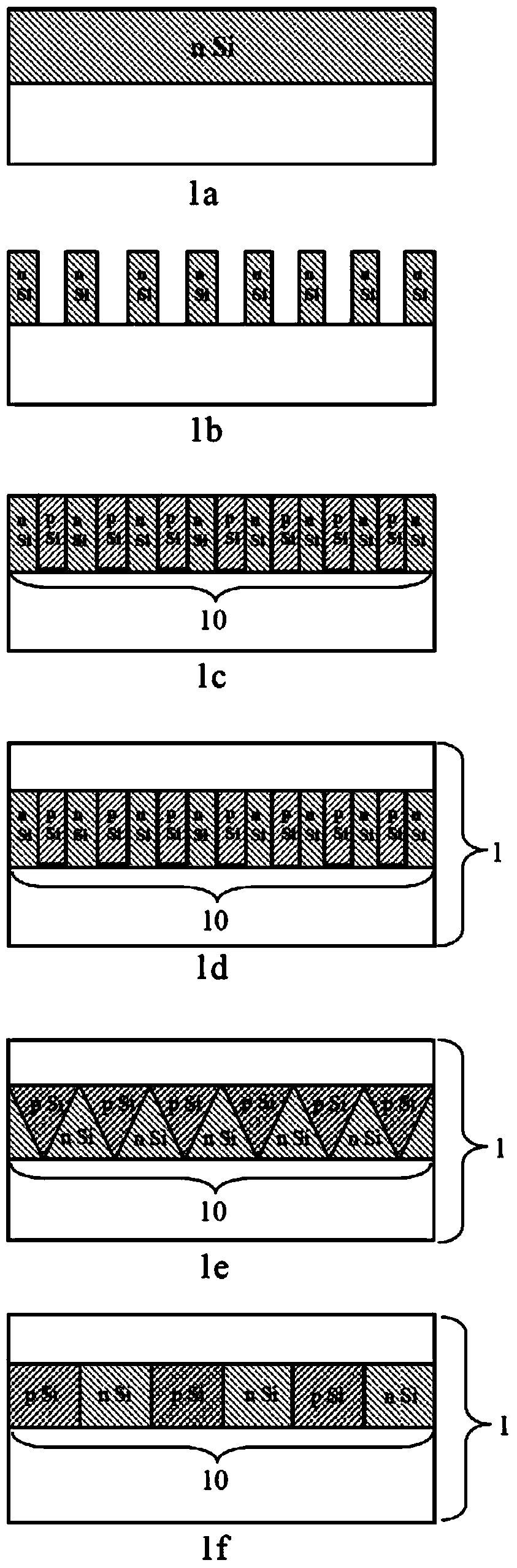
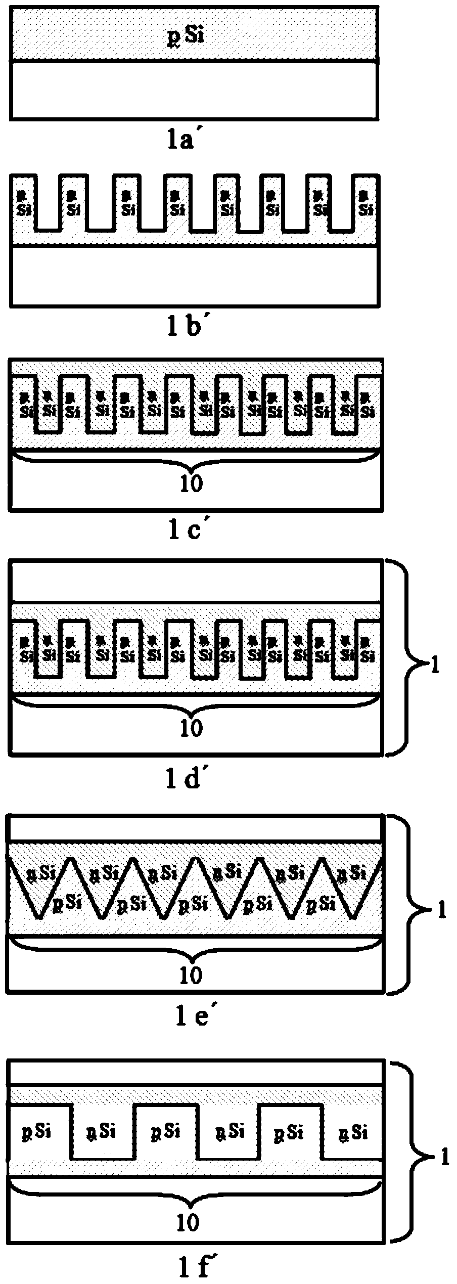
[0052] A nitride power transistor of the present invention comprises:

[0053] A silicon substrate comprising a differently doped semiconductor composite structure for forming a space charge depletion region;

[0054] a nitride nucleation layer on a silicon substrate;

[0055] a nitride buffer layer on the nitride nucleation layer;

[0056] a nitride channel layer on the nitride buffer layer;

[0057] A source and a drain are in contact with the nitride channel layer and a gate is located between the source and the drain.

[0058] Accordingly, a method for manufacturing a nitride power transistor includes:

[0059] Introducing a differently doped semiconductor composite structure in a silicon substrate to form a space charge depletion region;

[0060] growing a nitride nucleation layer on a silicon substrate containing a semiconductor composite structure;

[0061] growing a nitride buffer layer on the nitride nucleation layer;

[0062] growing a nitride channel layer on ...


PUM

PropertyMeasurementUnit
Heightaaaaaaaaaa

Abstract

The invention discloses a nitride power transistor and a manufacturing method thereof. The nitride power transistor comprises a silicon substrate, a nitride nucleating layer which is arranged on the silicon substrate, a nitride buffering layer which is arranged on the nitride nucleating layer, a nitride channel layer which is arranged on the nitride buffering layer, a source and a drain which are in contact with the nitride channel layer, and a grid which is arranged between the source and the drain, wherein the silicon substrate comprises a differently doped semiconductor composite structure which is used for forming a space charge depletion region. By introducing the differently doped semiconductor compound structure which can form the space charge depletion region in the silicon substrate of the nitride power transistor, the nitride power transistor is enabled to be able to withstand higher external voltage and the breakdown voltage of a device is improved.

Description

technical field [0001] The invention relates to the technical field of microelectronics, in particular to a nitride power transistor and a method for manufacturing the nitride power transistor. Background technique [0002] Gallium Nitride (GaN), the third-generation semiconductor material, has become a current research hotspot due to its large band gap, high electron saturation drift velocity, high breakdown field strength, and good thermal conductivity. In terms of electronic devices, gallium nitride materials are more suitable for manufacturing high-temperature, high-frequency, high-voltage and high-power devices than silicon and gallium arsenide, so gallium nitride-based electronic devices have good application prospects. [0003] In the past, gallium nitride power transistors were all made on sapphire or silicon carbide substrates. Due to the particularity of the gallium nitride heterojunction conductive channel and the limitation of process difficulty, the gallium nitr...

Claims


Application Information

Patent Timeline
IPC IPC(8): H01L29/06H01L29/778H01L21/335
CPCH01L29/0611H01L29/66431H01L29/7786H01L29/66462H01L29/0634H01L29/2003H01L21/02573H01L29/7783H01L21/02381H01L21/0254H01L29/7787
Inventor 程凯
Owner ENKRIS SEMICON
Why Eureka
Try Eureka