Component manufacturing method and component
A manufacturing method and component technology, which are applied in the manufacturing of components and the component field, can solve the problems of mechanical properties and electrical properties reduction, hinder the thinning of mounting parts, etc., and achieve the effect of cost reduction
- Summary
- Abstract
- Description
- Claims
- Application Information
AI Technical Summary
Problems solved by technology
Method used
Image

Examples
no. 1 approach )
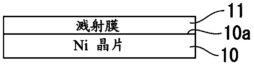
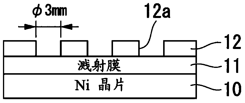
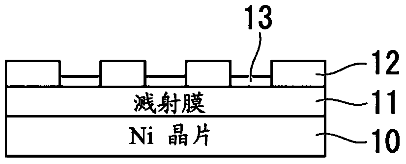
[0061] Figure 1A to Figure 1F It is a process sectional view explaining the manufacturing method of the component of this invention.
[0062] (step 1a)
[0063] First, if Figure 1A As shown, using a substrate 10 made of nickel (Ni) on one side 10a, an alloy film 11 containing silver (Ag), tin (Sn) and copper (Cu) is formed on one side 10a by sputtering. (Process A1).
[0064] As for the substrate 10 , one surface only needs to be formed of nickel. For example, a silicon (Si) substrate 10 formed with a nickel (Ni) film on one surface is suitably used. Hereinafter, a substrate having such a structure is also referred to as a Ni film-coated substrate 10 .
[0065] In particular, the present embodiment opposes the cathode electrode 60 (see image 3 ) and anode electrode 70 (see image 3 ), when the alloy film 11 is formed on one side of the substrate 10, a DC pulse voltage is applied to the cathode electrode 60, wherein the cathode electrode 60 is provided with silver (Ag)...
no. 2 approach
[0129] Next, a second embodiment of the present invention will be described.
[0130] In addition, in the following description, the part which differs from the said 1st Embodiment is mainly demonstrated, and the description of the part which is the same as the 1st Embodiment may be abbreviate|omitted.
[0131] Figure 6A to Figure 6F It is a process cross-sectional view explaining the manufacturing method of the component according to this embodiment.
[0132] (step 2a)
[0133] First, if Figure 6A As shown, using a substrate 10 formed of nickel (Ni) on one surface, an alloy film 11 containing silver (Ag), tin (Sn) and copper (Cu) is formed on the one surface by a sputtering method. (Process B1).
[0134] use as figure 2 In the shown device, a cathode electrode 60 and an anode electrode 70 are opposed to each other in a space of a reduced pressure atmosphere, and a DC pulse is applied to the cathode electrode 60 when the alloy film 11 is formed on one surface of the su...
Embodiment 1
[0150] Examples performed to confirm the effects of the present invention will be described.
PUM
| Property | Measurement | Unit |
|---|---|---|
| thickness | aaaaa | aaaaa |
| thickness | aaaaa | aaaaa |
Abstract
Description
Claims
Application Information
 - R&D Engineer
- R&D Manager
- IP Professional
- Industry Leading Data Capabilities
- Powerful AI technology
- Patent DNA Extraction
Browse by: Latest US Patents, China's latest patents, Technical Efficacy Thesaurus, Application Domain, Technology Topic.
© 2024 PatSnap. All rights reserved.Legal|Privacy policy|Modern Slavery Act Transparency Statement|Sitemap