
Method and device for detecting surface defects and thickness of semiconductor sheet material

A technology of thickness detection and detection method, applied in the direction of measuring device, using optical device, optical testing defect/defect, etc., can solve the problems of large influence of impurities and pollution, poor repeatability, unsuitable thickness of film, etc., to achieve repeatability High, easy to operate, low sample requirements

Active Publication Date: 2014-01-29
CHINA UNIV OF MINING & TECH
View PDF8 Cites 15 Cited by
  • Summary
  • Abstract
  • Description
  • Claims
  • Application Information

AI Technical Summary

Problems solved by technology

[0003] The purpose of the present invention is to solve the problems existing in the detection of surface defects and thickness of semiconductor sheets, and propose a method and device for detecting surface defects and thickness of semiconductor sheets that are easy to install, stable in test, and high in precision, so as to solve the problems of the prior art. Poor repeatability, high sample requirements, large impact of impurities and pollution, and unsuitable large slice thickness

Method used


Image

  • Method and device for detecting surface defects and thickness of semiconductor sheet material
  • Method and device for detecting surface defects and thickness of semiconductor sheet material
  • Method and device for detecting surface defects and thickness of semiconductor sheet material

Examples


Embodiment 1

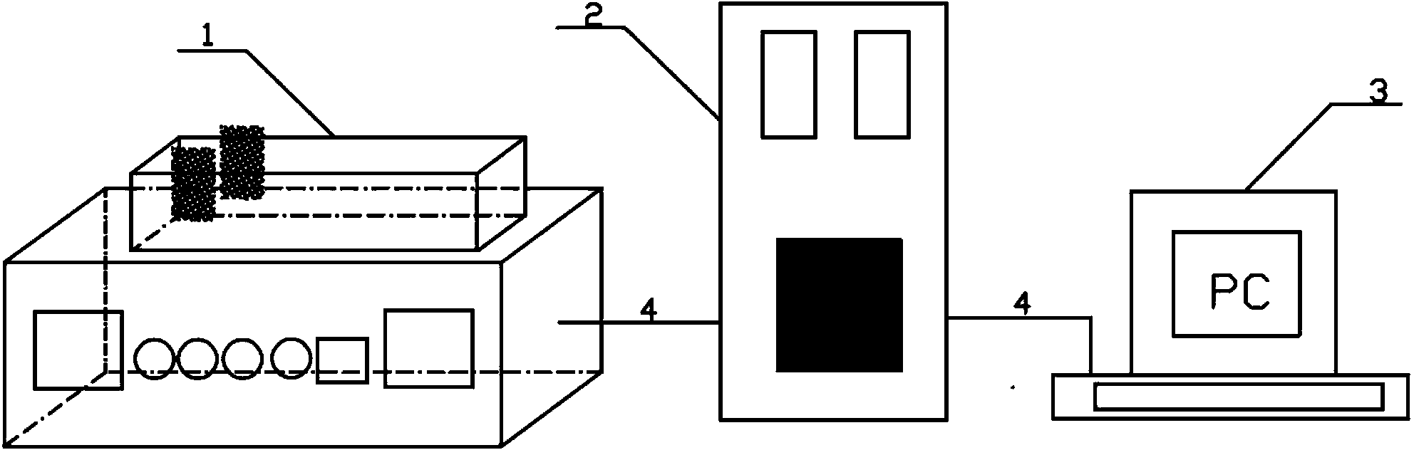
[0039] Embodiment 1: the present invention has the solution of detection method and device, and this detection device comprises frock 1, control cabinet 2, computer 3 and connecting cable 4, and frock 1, control cabinet 2 and computer 3 are connected in sequence by connecting cable 4 . figure 1 , figure 2 , image 3 and Figure 4 The solution of the detection method and device of the present invention is described.

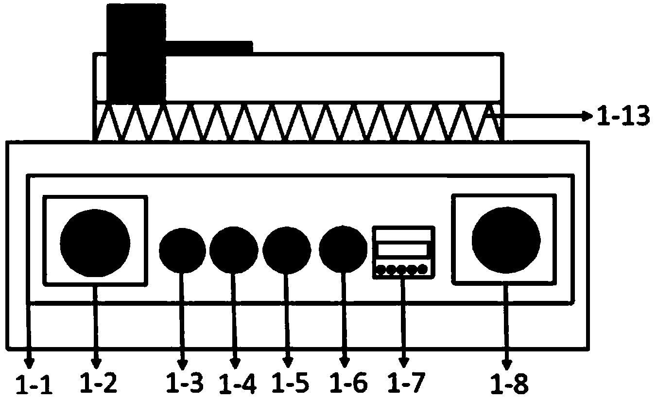
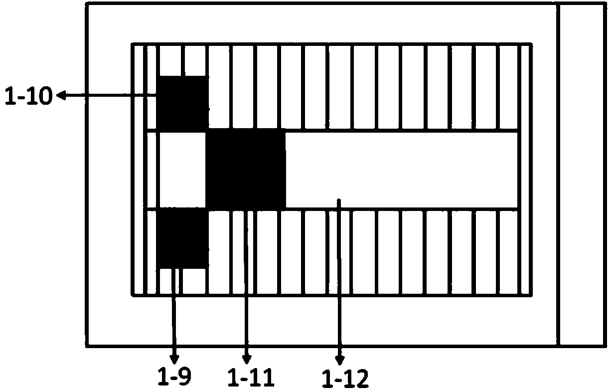
[0040] The tooling 1 includes: a control panel 1-1, a laser generator 1-9, a laser receiver 1-10, a test platform 1-12, a protection device 1-13, a synchronous operation system 1-15, a test platform support and Level adjustment system 1-16, power system 1-17 and base plate 1-19. All components of the tooling 1 are installed on the base plate 1-19, a control panel 1-1 is connected to the front of the tooling 1, and a laser generator 1-9, a laser receiver 1-10, and a test platform are connected to the upper end of the tooling 1 1-12 and the protection device 1...


PUM


Abstract

The invention provides a method and a device for detecting surface defects and thickness of a semiconductor sheet material and belongs to the method and the device for detecting the surface defects and the thickness of materials. According to the specific technical scheme adopted by the device, the device comprises a tool, a control cabinet, a computer and a connection cable, wherein the tool, the control cabinet and the computer are connected in sequence by the connection cable. The detection principle of the device is as follows: a green laser transmission principle is used for indirectly feeding back a height value signal of a plane sheet material and the surface defects and the thickness of the semiconductor sheet material are calculated by a series of formulas. The detection method comprises the following steps: a testing platform horizontal correction method, a synchronous operation method for a laser generator and a laser receiver, the detection method for the surface defects and the thickness of the semiconductor sheet material, a calculation method for the surface defects and the thickness of the semiconductor sheet material. The detection device is simple and practical, easy to operate, high in detection precision, good in repeatability, low in sample requirements and small in impurity and pollution influences, and is very suitable for scientific research requirements.

Description

technical field [0001] The invention relates to a method and device for detecting surface defects and thickness of materials, in particular to a method and device for detecting surface defects and thickness of semiconductor sheets. Background technique [0002] With the advancement of technology, semiconductors have been widely used in people's daily life. Due to the high requirements on the surface of the semiconductor sheet, its surface defects and thickness have a great influence on the subsequent preparation process and performance. Warpage changes, local hard spots, etc. before and after annealing can effectively improve the performance and efficiency of semiconductor sheets, and provide technical support for process improvement; at the same time, direct contact is generally not suitable for testing semiconductor sheets, so as not to cause semiconductor Scratches and contamination. At present, non-contact measurement methods include capacitance method, optical reflect...

Claims


Application Information

Patent Timeline
IPC IPC(8): G01N21/88G01B11/06
Inventor 黄飞闫爱华赵辉廖振华尹诗斌强颖怀张绍良
Owner CHINA UNIV OF MINING & TECH
Features
  • Generate Ideas
  • Intellectual Property
  • Life Sciences
  • Materials
  • Tech Scout
  • Unparalleled Data Quality
  • Higher Quality Content
  • 60% Fewer Hallucinations
Learn More