Base-region-gradient uni-traveling-carrier double-heterojunction phototransistor detector

A photosensitive transistor and double heterojunction technology, applied in semiconductor devices, electrical components, circuits, etc., can solve problems such as low hole mobility and limited photoelectric response speed of devices

Inactive Publication Date: 2014-01-29
BEIJING UNIV OF TECH
View PDF6 Cites 22 Cited by
  • Summary
  • Abstract
  • Description
  • Claims
  • Application Information

AI Technical Summary

Problems solved by technology

[0005] Most traditional HPTs use a single heterojunction epitaxial structure, using the base region and the collector region as the absorption region at the same time, the photogenerated carriers (including electrons and holes) are concentrated in the depletion region and the collector region, and the migration of holes The rate is low, and its slow transport in the collector region seriously limits the photoelectric response speed of the device, and there is a contradiction between the improvement of the responsivity and the response speed of the device.

Method used


Image

  • Base-region-gradient uni-traveling-carrier double-heterojunction phototransistor detector
  • Base-region-gradient uni-traveling-carrier double-heterojunction phototransistor detector
  • Base-region-gradient uni-traveling-carrier double-heterojunction phototransistor detector

Examples


Embodiment Construction

[0023] In order to make the object, technical solution and advantages of the present invention clearer, the present invention will be described in further detail below in conjunction with specific embodiments and with reference to the accompanying drawings.

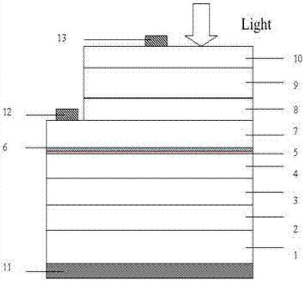
[0024] see figure 1 As shown, the InP / InGaAsP unidirectional carrier transport double heterojunction phototransistor (UTC-DHPT) detector provided by the embodiment of the present invention includes:

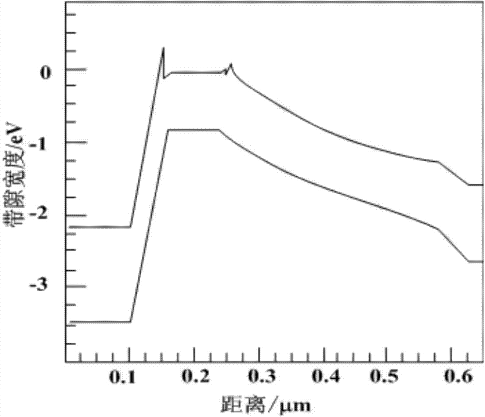
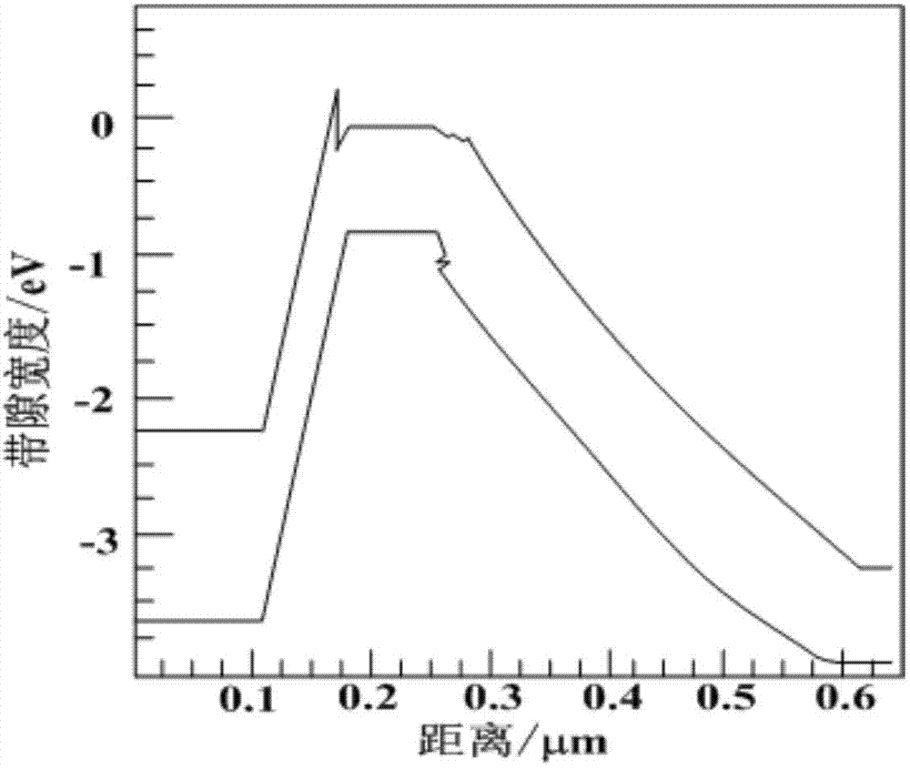
[0025] An InP substrate 1, on which an InP buffer layer 2, an InGaAsP sub-collector region 3, an InGaAsP collector region 4, InGaAsP transition layers 5 and 6, Material bandgap wavelength gradient InGaAsP base region 7, InP emitter region 8, InP cover layer 9, InGaAs ohmic contact layer 10; an emitter 13, made on the InGaAs ohmic contact layer by sputtering; a base 12, using The sputtering method is used to make it on the InGaAsP base region; a collector electrode 11 is made on the InP substrate by the sputtering method.

...


PUM


Abstract

The invention belongs to the technical field of semiconductor photoelectrons, and relates to a base-region-gradient uni-traveling-carrier double-heterojunction phototransistor (UTC-DHPT) detector capable of realizing high responsivity and high cut-off frequency. The detector comprises an InP substrate, an emitting electrode, a base electrode and a collector electrode; an InP buffer layer, an InGaAsP secondary collector region, an InGaAsP collector region, two InGaAsP transition layers different in material band gap wavelength, an InGaAsP base region gradient in material band gap wavelength, an InP emitting region, an InP cover layer and an InGaAs Ohmic contact layer are prepared on the InP substrate in sequence by the aid of a metal-organic chemical vapor deposition (MOCVD) method; the emitting electrode is produced on the InGaAs Ohmic contact layer by a sputtering method; the base electrode is produced on the InGaAsP base region through the sputtering method; the collector electrode is produced on the InP substrate through a vapor deposition method.

Description

technical field [0001] The invention belongs to the technical field of semiconductor optoelectronics, and is a unidirectional carrier transport double heterojunction photosensitive transistor (UTC-DHPT) detector capable of simultaneously realizing high responsivity and high cut-off frequency gradual change of the base region. Background technique [0002] The rapid growth of the business volume of the global broadband integrated network requires the optical communication network as the backbone network to have greater information transmission capacity and faster information processing speed. For the optical receiving end (Receiver), performances such as high speed, high responsivity, high gain and low noise are required. As a key device in the Receiver, the photodetector must have excellent detection efficiency and high-speed working ability. On the other hand, the current RoF system mostly adopts an intermediate frequency transmission scheme based on optical heterodyne, an...

Claims


Application Information

Patent Timeline
Patent Type & Authority Applications(China)
IPC IPC(8): H01L31/11H01L31/0352H01L31/0304
CPCH01L31/03529H01L31/1105
Inventor 霍文娟谢红云江之韵张良浩张万荣
Owner BEIJING UNIV OF TECH
Why Eureka
Try Eureka