Conductive film and method for producing same, and sputtering target used for same

A technology of a conductive film and a manufacturing method, which is applied in the field of sputtering targets, can solve the problems of the decline in the production yield of organic EL panels, the inability to obtain sufficient heat resistance, and the small surface roughness, so as to suppress defects and prevent the decline of the yield. , the effect of maintaining reflectivity

Active Publication Date: 2014-01-29
MITSUBISHI MATERIALS CORP
View PDF5 Cites 4 Cited by
  • Summary
  • Abstract
  • Description
  • Claims
  • Application Information

AI Technical Summary

Problems solved by technology

This leads to a decline in the production yield of organic EL panels
In addition, sulfur contained in the process atmosphere sulfides the Ag alloy film, and the sulfided region becomes a defect, which is also a cause of a decrease in yield.
In this way, it has not been possible to obtain an Ag alloy film with sufficient low resistance and high reflectivity, and also has a small surface roughness and high sulfide resistance.
In addition, when a conductive film is used as a reflective film of an LED, a reflective electrode film, etc., it is also required to maintain good reflectivity heat resistance against heat generated by the LED, but sufficient heat resistance cannot be obtained in the conventional Ag alloy film. heat resistance

Method used


Image

  • Conductive film and method for producing same, and sputtering target used for same
  • Conductive film and method for producing same, and sputtering target used for same

Examples


Embodiment

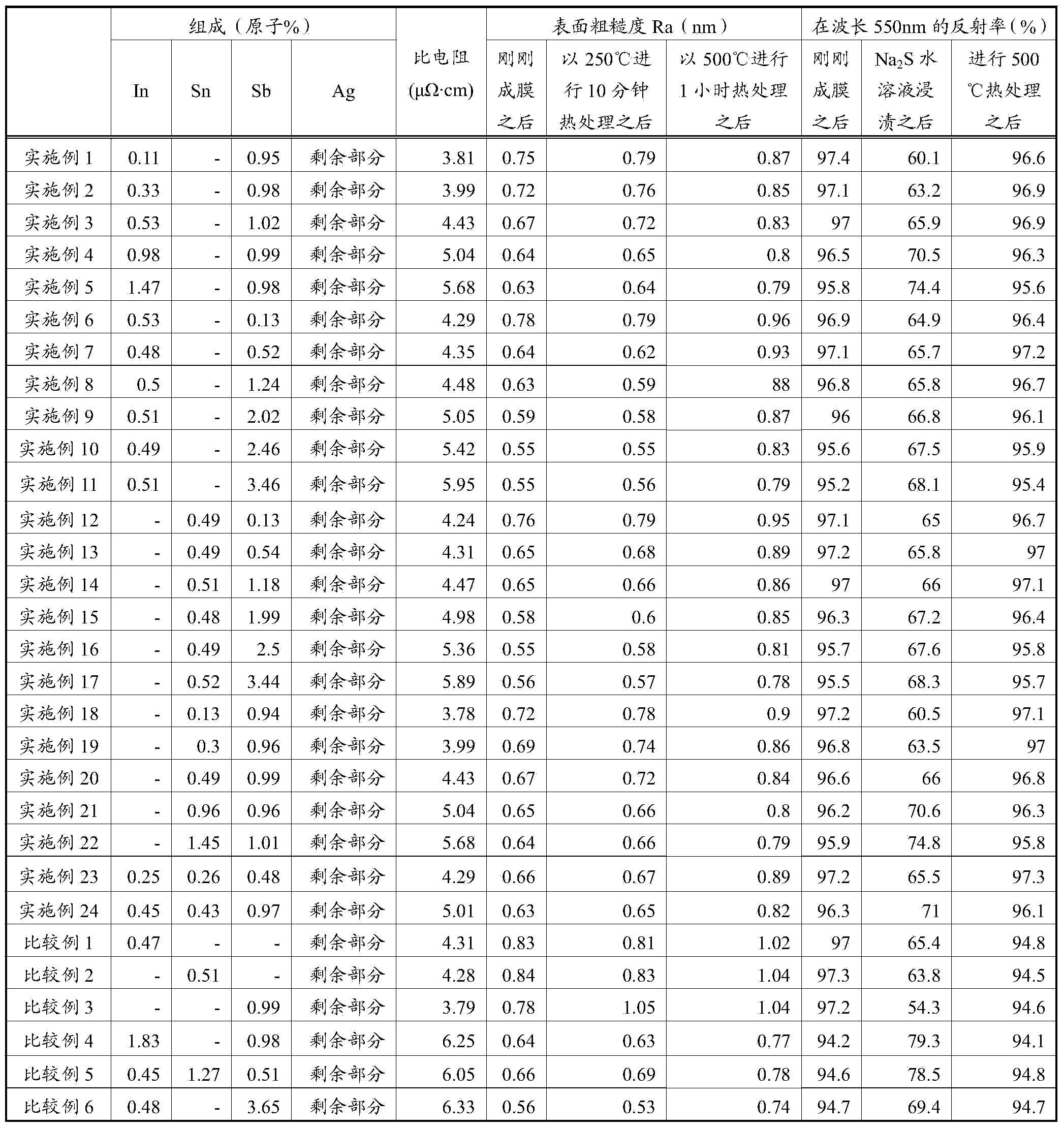
[0043] Hereinafter, the evaluation results of examples of the conductive film formed according to the above-mentioned embodiment will be described. First, in order to produce a sputtering target for a conductive film, Ag with a purity of 99.9% by mass or more, at least one of In and Sn with a purity of 99.9% by mass or more, and Sb are used as raw material powders so that they have a predetermined composition. weighing. Next, Ag is melted in a high vacuum or an inert gas atmosphere, and at least any one of In and Sn and Sb are added to the obtained molten metal in predetermined contents. Thereafter, melting is carried out in a vacuum or an inert gas atmosphere to manufacture a smelted ingot of an Ag alloy composed of the following components: the silver alloy contains 0.1 to 1.5 atomic % of at least one of In and Sn, and contains 0.1 to 3.5 The atomic % is Sb, and the rest is composed of Ag and unavoidable impurities.

[0044] Among them, the melting of Ag is carried out in ...


PUM

PropertyMeasurementUnit
diameteraaaaaaaaaa
thicknessaaaaaaaaaa
surface roughnessaaaaaaaaaa

Abstract

Provided are: a conductive film having low resistance and high reflectivity characteristics, and low surface roughness, and which combines high sulfidation resistance and heat resistance; a method for producing the conductive film; and a sputtering target used for the conductive film. The conductive film consists of a silver alloy having a component composition containing In and/or Sn at 0.1 to 1.5 at%, and further containing Sb at 0.1 to 3.5 at%, with the remainder comprising Ag and unavoidable impurities. The conductive film is suitable as a reflective electrode film for organic EL elements in which a transparent conductive film of an organic EL element is laminated on the surface, and an electroluminescent layer containing an organic EL layer is laminated thereabove.

Description

technical field [0001] The present invention relates to a conductive film suitable for reflective electrode films of organic electroluminescence (EL) elements and light emitting diodes (LEDs), wiring films of touch panels, and the like, and a method for producing the same, as well as a sputtering film used for the production method. target. Background technique [0002] Generally, in an organic EL display device, a structure is adopted in which an anode ( anode) and cathode (cathode) organic EL elements are formed in each pixel area. [0003] There are bottom emission methods for extracting light from the transparent substrate side and top emission methods for extracting light from the opposite side of the substrate among the light extraction methods of organic EL elements, and the top emission method with a high aperture ratio is advantageous for high brightness. In the past, in organic EL elements of the top emission method, a reflective electrode film of Al or Al alloy,...

Claims


Application Information

Patent Timeline
Patent Type & Authority Applications(China)
IPC IPC(8): H05B33/26C22C5/06C23C14/34G06F3/041H01B1/02H01L51/50H05B33/10
CPCH01B1/02H01L51/5218C22C5/06C23C14/3414C23C14/14H05B33/26H10K50/818C23C14/34G06F3/041H05B33/10H10K50/00
Inventor 野中庄平小见山昌三
Owner MITSUBISHI MATERIALS CORP
Why Eureka
Try Eureka