Alkaline type texturing process of monocrystalline silicon wafer
A single crystal silicon wafer, alkaline technology, applied in the field of solar cells, can solve the problems of inhomogeneous diffusion and difficult conductive paste, and achieve the effect of ensuring uniform diffusion, easier thickness control, and favorable coating.
- Summary
- Abstract
- Description
- Claims
- Application Information
AI Technical Summary
Problems solved by technology
Method used
Image

Examples
Embodiment 1
[0038] (a) Removing the damaged layer: the single crystal silicon wafer 1 was placed in a NaOH solution with a mass concentration of 12%, etched at 100°C for 45s, then washed with deionized water and dried.
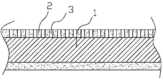
[0039] (b) Mask preparation: put the single crystal silicon wafer 1 with the damaged layer removed into an oxidation furnace to oxidize, and form SiO with a thickness of 10 nm on the surface of the single crystal silicon wafer 1 2 Mask 2.
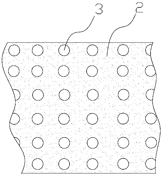
[0040] (c) Mask opening: for the formation of SiO 2 Laser window opening is carried out on the surface of the single crystal silicon wafer 1 of the mask 2, so that the SiO 2 Fenestration holes 3 evenly spaced are formed on the mask 2 (see figure 1 , figure 2 ), the fenestration interval is 8 μm, and the pore diameter is 4 μm.
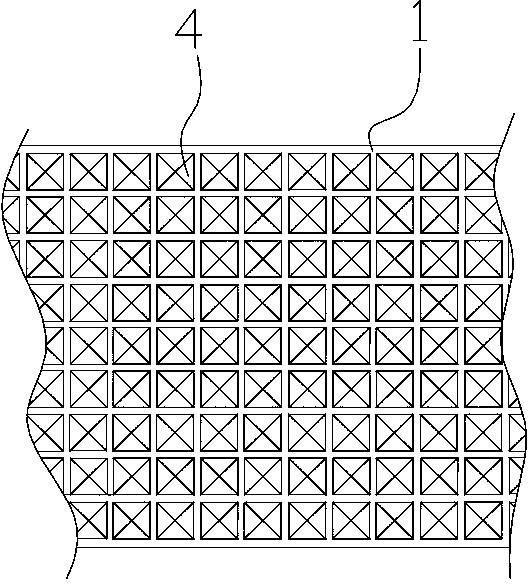
[0041] (d) Texturing the surface: Put the window-opened monocrystalline silicon wafer 1 in a NaOH solution with a mass concentration of 25%, and corrode it at 100°C for 60 minutes, so that the surface of th...
Embodiment 2
[0045] (a) Removing the damaged layer: the single crystal silicon wafer 1 was placed in a NaOH solution with a mass concentration of 16%, etched at 70°C for 30s, then washed with deionized water and dried.
[0046] (b) Mask preparation: put the single crystal silicon wafer 1 with the damaged layer removed into an oxidation furnace to oxidize, and form SiO with a thickness of 100 nm on the surface of the single crystal silicon wafer 1 2 Mask 2.
[0047] (c) Mask opening: for the formation of SiO 2 Laser window opening is carried out on the surface of the single crystal silicon wafer 1 of the mask 2, so that the SiO 2 Fenestration holes 3 evenly spaced are formed on the mask 2 (see figure 1 , figure 2 ), the window opening interval is 5m, and the aperture is 3m.
[0048] (d) Texturing the surface: place the windowed monocrystalline silicon wafer 1 in a NaOH solution with a mass concentration of 20, and etch at 80°C for 40 minutes to form an inverted pyramid-structured textu...
Embodiment 3
[0052] (a) Removing the damaged layer: the single crystal silicon wafer 1 was placed in a NaOH solution with a mass concentration of 13%, etched at 800°C for 50s, then washed with deionized water and dried.
[0053] (b) Mask preparation: put the single crystal silicon wafer 1 with the damaged layer removed into an oxidation furnace to oxidize, and form SiO with a thickness of 200 nm on the surface of the single crystal silicon wafer 1 2 Mask 2.
[0054] (c) Mask opening: for the formation of SiO 2 Laser window opening is carried out on the surface of the single crystal silicon wafer 1 of the mask 2, so that the SiO 2 Fenestration holes 3 evenly spaced are formed on the mask 2 (see figure 1 , figure 2 ), the fenestration interval is 4 μm, and the pore diameter is 2 μm.
[0055] (d) Texturing the surface: Place the window-opened monocrystalline silicon wafer 1 in an NaOH solution with a mass concentration of 18%, and corrode it at 70°C for 20 minutes, so that the surface of...
PUM
| Property | Measurement | Unit |
|---|---|---|
| Thickness | aaaaa | aaaaa |
| Thickness | aaaaa | aaaaa |
| Thickness | aaaaa | aaaaa |
Abstract
Description
Claims
Application Information
 - R&D
- Intellectual Property
- Life Sciences
- Materials
- Tech Scout
- Unparalleled Data Quality
- Higher Quality Content
- 60% Fewer Hallucinations
Browse by: Latest US Patents, China's latest patents, Technical Efficacy Thesaurus, Application Domain, Technology Topic, Popular Technical Reports.
© 2025 PatSnap. All rights reserved.Legal|Privacy policy|Modern Slavery Act Transparency Statement|Sitemap|About US| Contact US: help@patsnap.com