High-speed snspd with strong absorption structure and its preparation method

A strong absorption, high-speed technology, applied in the field of single-photon detection, can solve the problems of low yield and the decrease of intrinsic quantum efficiency of the detector, so as to reduce the probability of defects, ensure high-quality growth, and reduce the total length Effect

Active Publication Date: 2015-09-30
TSINGHUA UNIV
View PDF5 Cites 0 Cited by
  • Summary
  • Abstract
  • Description
  • Claims
  • Application Information

AI Technical Summary

Problems solved by technology

If you want to further increase the absorption rate, you need to increase the duty cycle or thickness of the nanowire, but the former puts forward more stringent requirements on sample preparation, while the latter will lead to a decrease in the intrinsic quantum efficiency of the detector.
US2012 / 0077680A1 "Nanowire-based detector" K.K.Berggren, X.Hu, D.Masciarelli et al. The method of increasing the absorption rate based on nano-antennas can be realized under the conditions of 4nm thick and 50% duty cycle NbN nanowires. The absorption rate is close to 100%, but this scheme also puts forward relatively high requirements on sample preparation, and the final experimental results show that its yield is not high

Method used


Image

  • High-speed snspd with strong absorption structure and its preparation method
  • High-speed snspd with strong absorption structure and its preparation method
  • High-speed snspd with strong absorption structure and its preparation method

Examples


Embodiment Construction

[0024] The present invention will be described in further detail below with reference to the accompanying drawings and embodiments.

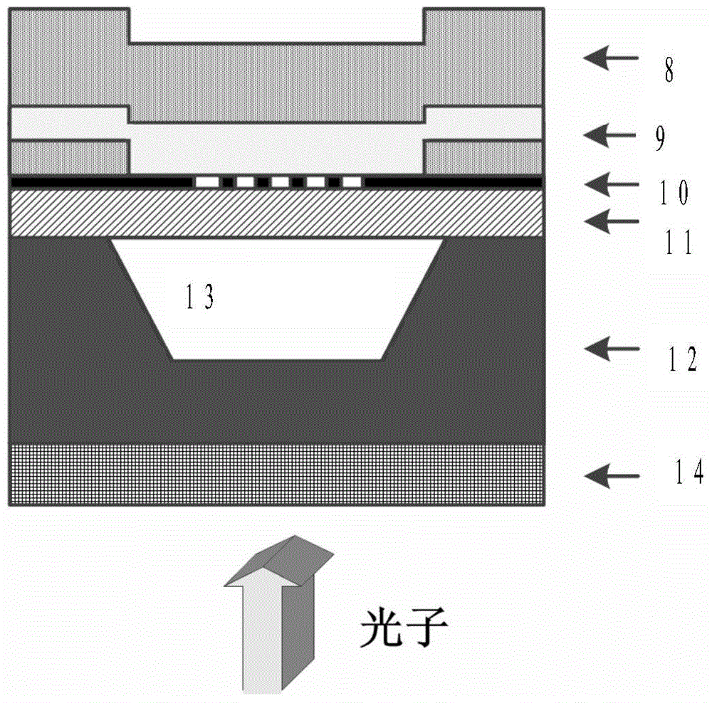
[0025] The present invention provides a comparative SNSPD called "first structure", and the SNSPD of the present invention is called "second structure".

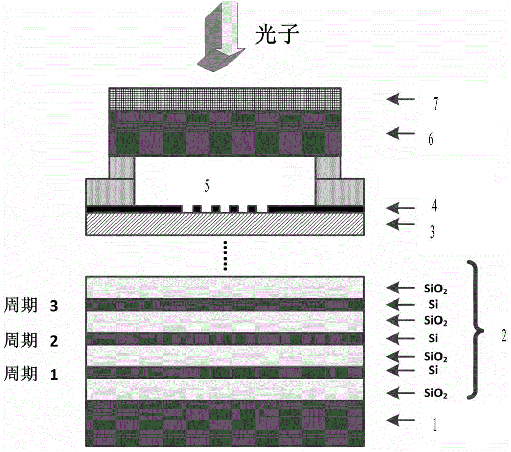
[0026] like figure 1 Shown is the first superconducting nanowire single-photon detector with a strong absorption structure, including an underlying Si substrate-1 on which multiple layers of Si / SiO are deposited 2 The Bragg reflector 2 is formed by periodic arrangement. The top of the Bragg reflector 2 is provided with a bottom resonant cavity-3 formed by epitaxial single crystal Si, and above the bottom resonator cavity-3 there are superconducting nanowires-4, superconducting nanowires-4 There is an upper air resonant cavity 5 thereon, a Si chip 6 is arranged above the upper air resonant cavity 5, and an anti-reflection film-7 is arranged on the Si chip 6.

[0027] Made of multilayer Si / SiO...


PUM


Abstract

A high-speed SNSPD with a strong absorption structure and a preparation method thereof. The SNSPD is based on a high-refractive index incident medium and an air cavity structure, which can further increase the photon absorption rate of superconducting nanowires. Compared with the prior art, the present invention uses the same material and Under the condition of thick superconducting ultra-thin films made into nanowires, the absorption rate close to 100% can be achieved with a lower duty cycle, which greatly reduces the difficulty of the electron beam exposure step, especially for ultra-fine nanowires It is more favorable for the preparation of the superconducting film, and the use of SOI substrate can ensure the high-quality growth of the superconducting film at the same time, without affecting the intrinsic quantum efficiency of the detector. In addition, under the condition of ensuring the same large effective detection area, Since the total length of the required nanowires is significantly reduced, the maximum count rate of the detector can be increased, and the probability of defects occurring during the fabrication process is significantly reduced.

Description

technical field [0001] The invention belongs to the field of single-photon detection, is suitable for realizing ultra-fast and high-efficiency single-photon detection in the near-infrared band, and relates to a high-speed SNSPD with a strong absorption structure and a preparation method thereof. Background technique [0002] In recent years, G.N.Gol'tsman et al., "Picosecond superconducting single-photon optical detector," Applied Physics Letter, vol.79, pp.705–707, 2001. The Superconducting Nanowire Single Photon Detector (SNSPD) , due to its excellent single-photon detection capability, ultra-high count rate, low dark count, and small time jitter in the visible and infrared bands, it has attracted more and more attention, especially in the near-infrared band. Both the efficiency and the highest count rate have surpassed the existing avalanche photodiodes based on compound semiconductor materials, making them the most powerful candidate detectors in the fields of quantum co...

Claims


Application Information

Patent Timeline
Patent Type & Authority Patents(China)
IPC IPC(8): H01L31/08H01L31/0352H01L31/18G01J1/42
CPCG01J1/4204B82Y30/00B82Y40/00H10N60/83H10N60/80H10N60/30Y02P70/50
Inventor 成日盛刘建设李铁夫陈炜
Owner TSINGHUA UNIV
Why Eureka
Try Eureka