How to form a mos transistor

A MOS transistor and body region technology, which is applied in the fields of semiconductor devices, semiconductor/solid-state device manufacturing, electrical components, etc., can solve the problems of increasing the volume of MOS transistors and reducing the feature size of transistors, and achieves improved electrical performance and improved tunability. The effect of range and stability

Active Publication Date: 2016-01-06
SEMICON MFG INT (SHANGHAI) CORP
View PDF7 Cites 0 Cited by
  • Summary
  • Abstract
  • Description
  • Claims
  • Application Information

AI Technical Summary

Problems solved by technology

[0006] However, as the feature size of transistors continues to decrease, changing the thickness of the sidewall will undoubtedly increase the volume occupied by the MOS transistor, which is not conducive to the reduction of the feature size of the transistor.

Method used


Image

  • How to form a mos transistor
  • How to form a mos transistor
  • How to form a mos transistor

Examples


Embodiment Construction

[0015] In order to make the above objects, features and advantages of the present invention more comprehensible, specific implementations of the present invention will be described in detail below in conjunction with the accompanying drawings.

[0016] In the following description, many specific details are set forth in order to fully understand the present invention, but the present invention can also be implemented in other ways than those described here, so the present invention is not limited by the specific embodiments disclosed below.

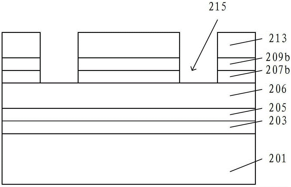
[0017] As mentioned in the background technology section, existing semiconductor devices contain a plurality of NMOS transistors and PMOS transistors. Due to different manufacturing processes, the threshold voltages of the manufactured NMOS transistors and PMOS transistors are not the same, which in turn leads to different devices inside the semiconductor device. Compatible or fabricated semiconductor devices are not compatible with other ...


PUM


Abstract

A method for forming an MOS transistor comprises providing a substrate; forming a back gate electrode, a back gate dielectric layer, a body region, a first functional layer and a front gate dielectric layer sequentially from the bottom surface of the substrate, the first functional layer being used for increasing the rate of migration of a carrier in a channel region; etching the front gate dielectric layer and the first functional layer and forming a first groove exposing a portion of the body region; conducting ion implantation on the first groove along the body region to form a heavily doped region; filling a metal layer in the first groove and forming a plug connected with the heavily doped region; and forming a second functional layer and a front gate on the surface of a front gate dielectric layer between the heavily doped regions sequentially from the bottom to the top, the second functional layer being used for reducing the leakage current of the channel region. The method for forming the MOS transistor can adjust the threshold voltage of the formed MOS transistor, improve the compatibility and matching rate of each MOS transistor in semiconductor devices and improve the performance of formed semiconductor devices.

Description

technical field [0001] The invention relates to the technical field of semiconductor manufacturing, in particular to a method for forming a MOS transistor. Background technique [0002] With the continuous development of modern high-tech industries represented by electronic communication technology, the total output value of the world's integrated circuit industry is growing at a rate of 30% every year. Static random access memory is an important component in integrated circuits, which has small size and high density. Among semiconductor memory devices, Static Random Access Memory (SRAM) has advantages of lower power consumption and faster operation speed than Dynamic Random Access Memory (DRAM) devices. Static random access memory can easily locate the physical unit through the bitmap test equipment to study the effective mode of the product. In addition, the yield rate of the SRAM can be used as an important index to measure the yield rate of the whole process of a semic...

Claims


Application Information

Patent Timeline
Patent Type & Authority Patents(China)
IPC IPC(8): H01L21/336
CPCH01L29/1033H01L29/24H01L29/42364H01L29/66484
Inventor 张海洋王新鹏
Owner SEMICON MFG INT (SHANGHAI) CORP
Why Eureka
Try Eureka