Strain gauge and preparation method of silicon germanium heterojunction nanowire array as sensitive element
A silicon germanium heterojunction, nanowire array technology, applied in nanotechnology, nanotechnology, nanotechnology for sensing, etc., can solve the problems of surface state reduction, reduce piezoresistive effect, etc., and achieve piezoresistive coefficient. Large, reduced resistance, improved sensitivity and improved noise immunity
- Summary
- Abstract
- Description
- Claims
- Application Information
AI Technical Summary
Problems solved by technology
Method used
Image
Examples
preparation example Construction
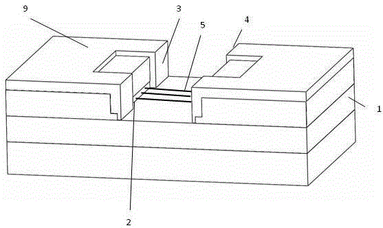
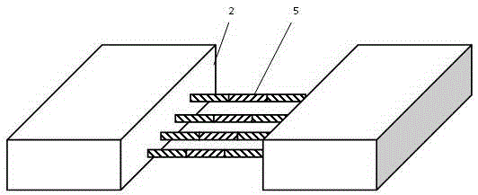
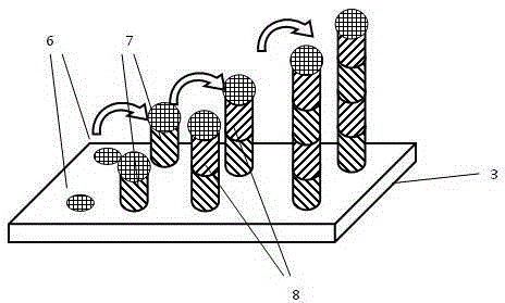
[0037] The above-mentioned silicon germanium heterojunction nanowire array is used as a method for preparing a strain gauge of a sensitive element, comprising the following steps:
[0038] In the first step, a protective oxide layer is formed on the upper surface of the silicon-on-insulator wafer 1 by a thermal oxidation method, and a silicon-on-insulator wafer with an oxide layer is produced;
[0039]The second step is to open deep grooves: through photolithography and reactive ion etching methods, deep grooves are opened on the silicon-on-insulator wafer with an oxide layer prepared in the first step.
[0040] The second step specifically includes the following processes: step 201), such as Figure 4 As shown, a reactive ion etching process is used to etch and form deep grooves on the silicon-on-insulator wafer 1, so that the silicon layer in the silicon-on-insulator wafer 1 is left with a thickness of 300-500 nanometers; step 202), as Figure 5 As shown, using a thermal ox...
Embodiment
[0050] Utilize above-mentioned preparation method to prepare strain gauge:
[0051] 1) Prepare SOI substrate: select P-type heavily doped device layer SOI substrate, in which the thickness of the device layer is 1.6 microns, the resistivity is less than 0.1Ω*cm, and the buried oxide layer is 2.0 microns;
[0052] 2) Thermal oxidation: obtain an oxide layer with a thickness of 600 nm on the surface of the SOI substrate;
[0053] 3) Photolithography: remove the oxide layer between the first sidewall 3 and the second sidewall 4;
[0054] 4) Reactive ion etching: deep grooves are opened on the SOI substrate. At this time, the device layer is still 400 nanometers thick; the first sidewall 3 and the second sidewall 4 on the SOI substrate are separated by deep grooves ;
[0055] 5) The second thermal oxidation: an oxide layer with a thickness of 200 nanometers is obtained, and the thickness of the device layer is 300 nanometers;
[0056] 6) Photolithography: remove the oxide layer...
PUM
 Abstract
Description
Claims
Application Information


