Wet etching method in multilayer metal patterning process

A multi-layer metal and wet etching technology, which is applied in the direction of electrical components, semiconductor/solid-state device manufacturing, semiconductor devices, etc., can solve problems such as device failure, increased stress on silicon wafers, and poor reliability, so as to reduce costs and improve efficiency , the effect of improving quality

Active Publication Date: 2014-03-26
CSMC TECH FAB2 CO LTD
View PDF3 Cites 12 Cited by
  • Summary
  • Abstract
  • Description
  • Claims
  • Application Information

AI Technical Summary

Problems solved by technology

[0003] The shortcoming of above-mentioned electroless silver plating, aluminum sintering and evaporation process method preparation electrode method is: chemical silver plating process stability is not good, and silicon-silver alloy easily causes silicon chip internal stress to increase, and reliability is poor, especially larger area silicon chip alloy When the stress and deformation are large, it will lead to cracking of the silicon chip and make the device invalid.
[0005] However, the existing Ag-Ni-Ti-Al-TiN-Ti multi-layer metal patterning process generally uses Lift-Off technology for patterning. When the Lift-Off process processes multi-layer metal structures, it needs to use two laser Engraving, which greatly increases the cost of the patterning process

Method used


Image

  • Wet etching method in multilayer metal patterning process
  • Wet etching method in multilayer metal patterning process
  • Wet etching method in multilayer metal patterning process

Examples


Embodiment Construction

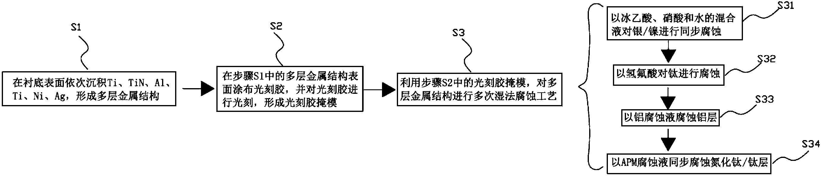
[0032] As mentioned in the background technology, in the existing multi-layer metal patterning process, the Lift-Off technology is generally used, and this process requires two photolithography, that is, the first photolithography of the Al layer and the Lift-Off The second lithography in . Therefore, the process complexity and cost of the existing multi-layer metal patterning process have greatly affected the development of the semiconductor multi-layer metal process.

[0033] According to the above situation, the present invention proposes a new multi-layer metal patterning process. The multi-layer metallization process only needs one photolithography technology, and then cooperates with multiple wet etching processes to pattern the multi-layer metal, greatly The complexity and cost of the patterning process are reduced.

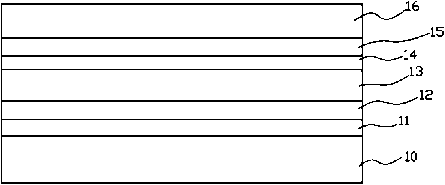
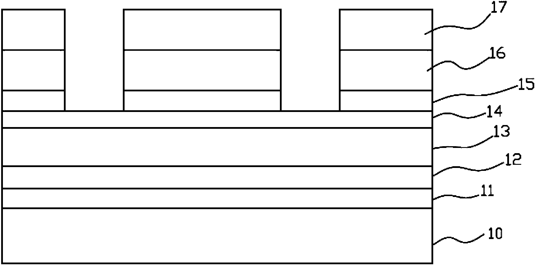
[0034] See figure 1 , figure 1 It is a flow chart of the steps of the multi-layer metal patterning process of the present invention. As shown in the fi...


PUM

PropertyMeasurementUnit
thicknessaaaaaaaaaa

Abstract

The invention provides a wet etching method in the multilayer metal patterning process. According to the method, etching is performed on Ag and Ni by utilizing the mixed liquor of glacial acetic acid (CH3COOH), nitric acid (HNO3) and water, etching is performed on Ti by utilizing diluted hydrofluoric acid, etching is performed on Al by utilizing an Al etching solution, and finally, etching is performed on TiN and Ti by utilizing an APM solution. According to the invention, the photoetching process needs only once, so the cost is greatly reduced, and the advantage of good etching window morphology control can be realized in all wet etching steps, so the quality of the patterning process can be improved, and Ag, Ni, Al as well as TiN and Ti are etched in one step separately, so the flow of the wet etching process can be simplified, and the efficiency of the process can be improved.

Description

technical field [0001] The invention relates to a semiconductor patterning process, in particular to a wet etching method for realizing a multilayer metal structure by photolithography at one time. Background technique [0002] At present, most semiconductor devices use silicon single crystal as the substrate. After diffusion and other production processes, one or several PN junctions are formed in the silicon wafer according to the design. However, silicon is a non-metallic semiconductor and is not easy to connect to external circuits. Traditionally, the external lead wires of semiconductor devices are connected to the silicon chip. Generally, two methods are used according to the structure of the device, namely welding type and crimping type. The welding type uses chemical silver plating process to form a silver layer electrode on the surface of the silicon chip, and then uses lead Solder such as tin is connected to the external lead by welding; the crimping type is proces...

Claims


Application Information

Patent Timeline
Patent Type & Authority Applications(China)
IPC IPC(8): H01L21/28
CPCH01L21/32134
Inventor 韩文胜缪新海臧延亮
Owner CSMC TECH FAB2 CO LTD
Why Eureka
Try Eureka