Xenon difluoride gas-phase etching method for barrier layer

A technique for etching barrier layers and xenon difluoride, which is applied in the fields of electrical components, semiconductor/solid-state device manufacturing, circuits, etc., can solve problems such as excessive etching of the barrier layer 23, and achieve improved etching uniformity and good process effects , the effect of increasing the etching rate

Active Publication Date: 2014-04-02
ACM RES SHANGHAI
View PDF2 Cites 6 Cited by
  • Summary
  • Abstract
  • Description
  • Claims
  • Application Information

AI Technical Summary

Problems solved by technology

Therefore, in order to increase the rate of xenon difluoride gas phase etching, the semiconductor structure will be heated, while the traditional heating method is contact heating, so that the temperature of the entire semiconductor structure is exactly the same, xenon difluoride gas phase etching low K dielectric The barrier layer 23 on the layer 22 and the barrier layer 23 on the sidewall of the trench and the connection hole are the same, which will also cause excessive etching of the barrier layer 23 on the sidewall of the trench and the connection hole

Method used


Image

  • Xenon difluoride gas-phase etching method for barrier layer
  • Xenon difluoride gas-phase etching method for barrier layer
  • Xenon difluoride gas-phase etching method for barrier layer

Examples


Embodiment Construction

[0024] In order to describe the technical content, achieved goals and effects of the present invention in detail, the following will be described in detail in conjunction with the embodiments and accompanying drawings.

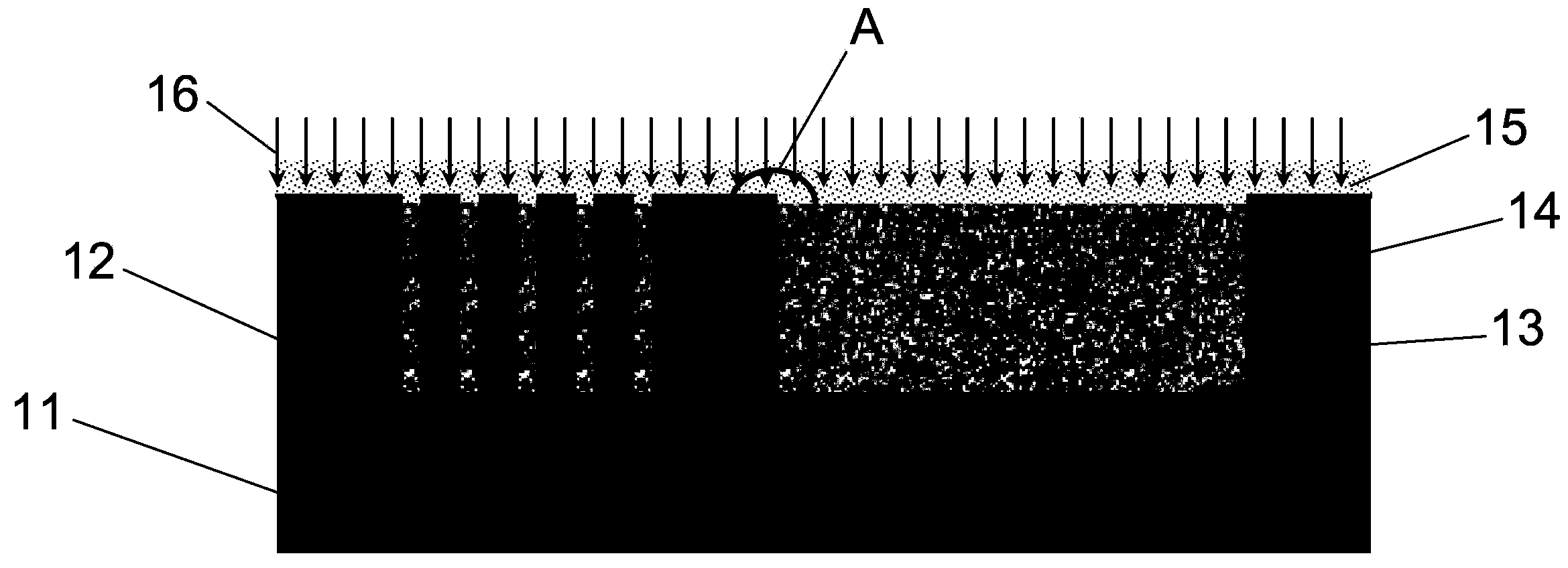
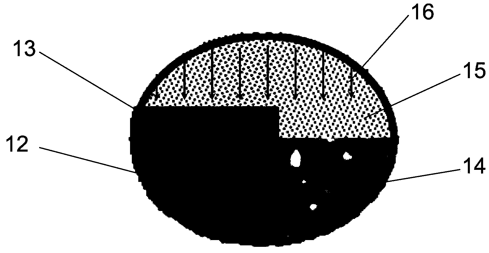
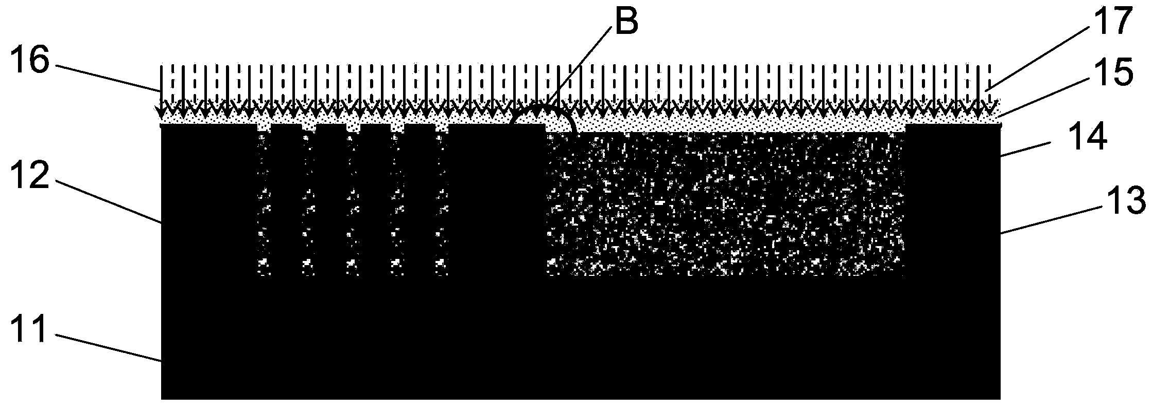
[0025] The present invention relates to xenon difluoride (XeF 2 ) method of vapor phase etching barrier layer.

[0026] see figure 1 and figure 2 , is a schematic cross-sectional structure diagram of an embodiment of the xenon difluoride gas-phase etching barrier layer of the present invention, disclosing a method of the gas-phase etching barrier layer of xenon difluoride of the present invention. Before introducing the method for gas-phase etching barrier layer of xenon difluoride of the present invention in detail, the manufacturing process of the metal interconnection line is briefly introduced, including the following steps: first, a semiconductor substrate 11 is provided, and a low K dielectric layer 12; secondly, form trenches and connection holes o...


PUM


Abstract

The invention discloses a xenon difluoride gas-phase etching method for a barrier layer. The method comprises the following steps: (1) spraying xenon difluoride to the surface of an exposed barrier layer; (2) only irradiating the barrier layer on the upper surface of a dielectric layer to increase the etching rate of the barrier layer on the upper surface of the dielectric layer to be higher than that of the barrier layer on the sidewalls of grooves and connecting holes by adopting light beams. According to the method, the barrier layer on the upper surface of the dielectric layer is irradiated by the light beams to increase the etching rate of the barrier layer on the upper surface of the dielectric layer to be higher than that of the barrier layer on the sidewalls of the grooves and the connecting holes, so that the barrier layer on the sidewalls of the grooves and the connecting holes is prevented from being excessively etched, the microcosmic etching uniformity is improved, and better process effects are achieved.

Description

technical field [0001] The invention relates to the technical field of integrated circuit device manufacturing, and more specifically, relates to a method for etching a barrier layer in the gas phase of xenon difluoride. Background technique [0002] As the size of integrated circuit devices continues to shrink, interconnection delays have increasingly become a bottleneck problem restricting the development of integrated circuits. In order to reduce the interconnection delay, in the manufacture of metal interconnection lines of integrated circuit devices, metal copper with a lower resistivity is used instead of aluminum with a higher resistivity to reduce the interconnection resistance, and a low-K dielectric is selected. material to reduce the capacitance between metal interconnect lines. Such as Figure 6 and Figure 7 As shown, the manufacturing process of the metal interconnection generally includes: firstly, forming a low-K dielectric layer 22 on the semiconductor sub...

Claims


Application Information

Patent Timeline
Patent Type & Authority Applications(China)
IPC IPC(8): H01L21/768H01L21/3213
CPCH01L21/32135H01L21/76865
Inventor 王坚贾照伟王晖
Owner ACM RES SHANGHAI
Why Eureka
Try Eureka