Patterned electrode preparation method

A patterned electrode and patterned technology, applied in the direction of circuits, photovoltaic power generation, electrical components, etc., can solve the problems of expensive, low-efficiency preparation methods, and no separation of graphics, and achieve easy promotion and use, effective preparation methods, and neat edges Effect

Inactive Publication Date: 2014-04-02
未名光电盐城有限公司 +1
View PDF0 Cites 8 Cited by
  • Summary
  • Abstract
  • Description
  • Claims
  • Application Information

AI Technical Summary

Problems solved by technology

[0003] This traditional method is usually done in a yellow light clean room. The thickness of the glue film is controlled by the speed and time of the glue application. The glue must be uniform to ensure the integrity of the prepared electrode pattern. During the glue application process, there must be no dirty spots. Bubbles, otherwise the pattern will be missing; exposure needs to transfer the mask pattern to the substrate, different electrode patterns need different masks, the exposure process needs to control the exposure amount and time to adjust the photoresist degree of sensitivity If there is too much, the graphics will be washed away after development, and if the photosensitive is too little, the graphics will not be separated; the developer needs to be used in conjunction with the photoresist, and the development time should be well controlled, otherwise there will be less and over-display phenomena; therefore, the existing preparation The method of patterning electrodes not only requires more expensive gluing, exposure, and development equipment, but also requires corresponding process control, that is, this preparation method has low efficiency, high cost, and poor operability.

Method used


Image

  • Patterned electrode preparation method
  • Patterned electrode preparation method
  • Patterned electrode preparation method

Examples


Embodiment 1

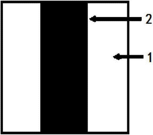
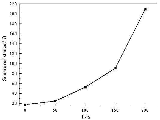
[0025] Use the UV inkjet printer to print the protective film corrosion method, respectively corrode the electrodes on the 25×25mm ITO conductive substrate, the size is 10×25mm, such as figure 1 As shown, the black area is the ITO electrode. The corrosion time was 50 s, 100 s, 150 s, and 200 s, and the corrosion solution was prepared by mixing 36% hydrochloric acid, 98% nitric acid, and deionized water at a volume ratio of 10:0.8:10. Formed, using the sheet resistance tester to measure the sheet resistance of the electrode under different corrosion times, such as figure 2 As shown, the change trend of the sheet resistance with time, and a patterned ITO electrode can be obtained between 50 s and 200 s, and the edges of the graph are neat, such as image 3 As shown, the figure is a 500-fold micrograph. It can be seen from the figure that at the corroded interface of the ITO electrode, the edge is still very clear when magnified by a microscope 500 times, without jaggedness...

Embodiment 2

[0027] Substrates (25×25mm) with ITO conductive electrodes (10×25mm) were prepared by photoresist mask and UV inkjet printer printing protective film corrosion method, and the structure was prepared on this basis: glass / ITO (180nm) / NPB(50nm) / DCM: (Alq3 0.5% 20nm) / Alq3(30nm) / Ca(10nm) / Ag OLED device, in which ITO is the anode, NPB is the hole transport layer, DCM is the light emitting layer, Alq3 is the electron transport layer, Ca is the buffer layer, and Ag is the cathode. Among them, the ITO electrodes of group A devices are prepared by photolithography etching, and the ITO electrodes of group B devices are prepared by UV inkjet printer printing protective film corrosion method. The specific process is as follows:

[0028] (1) The substrates of group A and B devices are glass with ITO electrodes. Firstly, the substrates are scrubbed and cleaned. The size is 10×25mm;

[0029] (2) Place the processed device substrates of groups A and B in a multi-source organic molecular vapo...


PUM


Abstract

The invention belongs to the field of organic electronic devices and particularly relates to a patterned electrode preparation method. The invention adopts the technical scheme as follows: an electrode pattern protection film with oil ink is printed on the substrate of an electrode by a UV flat inkjet printer, the substrate is put into a corrosive liquid to corrode the electrode not protected by the oil ink on the substrate so as to form the patterned electrode on the substrate, the oil ink is removed through ultrasonic washing with the help of deionized water and an alkaline solution, then the patterned electrode is prepared, and the organic electronic device is further prepared on the patterned electrode. The patterned electrode prepared through the method provided by the invention has tidy edges, is not zigzag and simple in operation and does not need special process or equipment, and the patterned electrode preparation method is suitable for manufacturing a metal oxide electrode commonly used for a semiconductor device, and popularization and application are facilitated.

Description

technical field [0001] The invention belongs to the field of organic electronic devices, and in particular relates to a method for preparing a patterned electrode. Background technique [0002] The patterning of transparent electrodes of organic electronic devices is usually prepared by the traditional wet etching method. The traditional electrode patterning method is to spin-coat (print) photoresist on the conductive film, and then pre-baking, exposing, developing, and hardening the film. After the photolithography process, the patterning of the protective layer is formed, and then the semiconductor substrate to be etched with the pattern of the protective layer is immersed in an etching solution controlled within a certain temperature range for etching. Finally, rinse the taken out semiconductor substrate with deionized water, put it into a stripping solution to remove the glue, and then process it again to obtain a patterned electrode. [0003] This traditional method is...

Claims


Application Information

Patent Timeline
Patent Type & Authority Applications(China)
IPC IPC(8): H01L51/56
CPCH10K71/611H10K71/621Y02E10/549Y02P70/50
Inventor 刘屹东沈波涛张乐乐陈志宽黄维
Owner 未名光电盐城有限公司
Why Eureka
Try Eureka