Preparation method for copper indium gallium diselenide thin film
A copper indium gallium selenide thin film technology, applied in the field of preparation of copper indium gallium selenide thin film, can solve the problems of small grain size, poor quality of copper indium gallium selenide thin film, short film growth time, etc.
- Summary
- Abstract
- Description
- Claims
- Application Information
AI Technical Summary
Problems solved by technology
Method used
Image

Examples
preparation example Construction
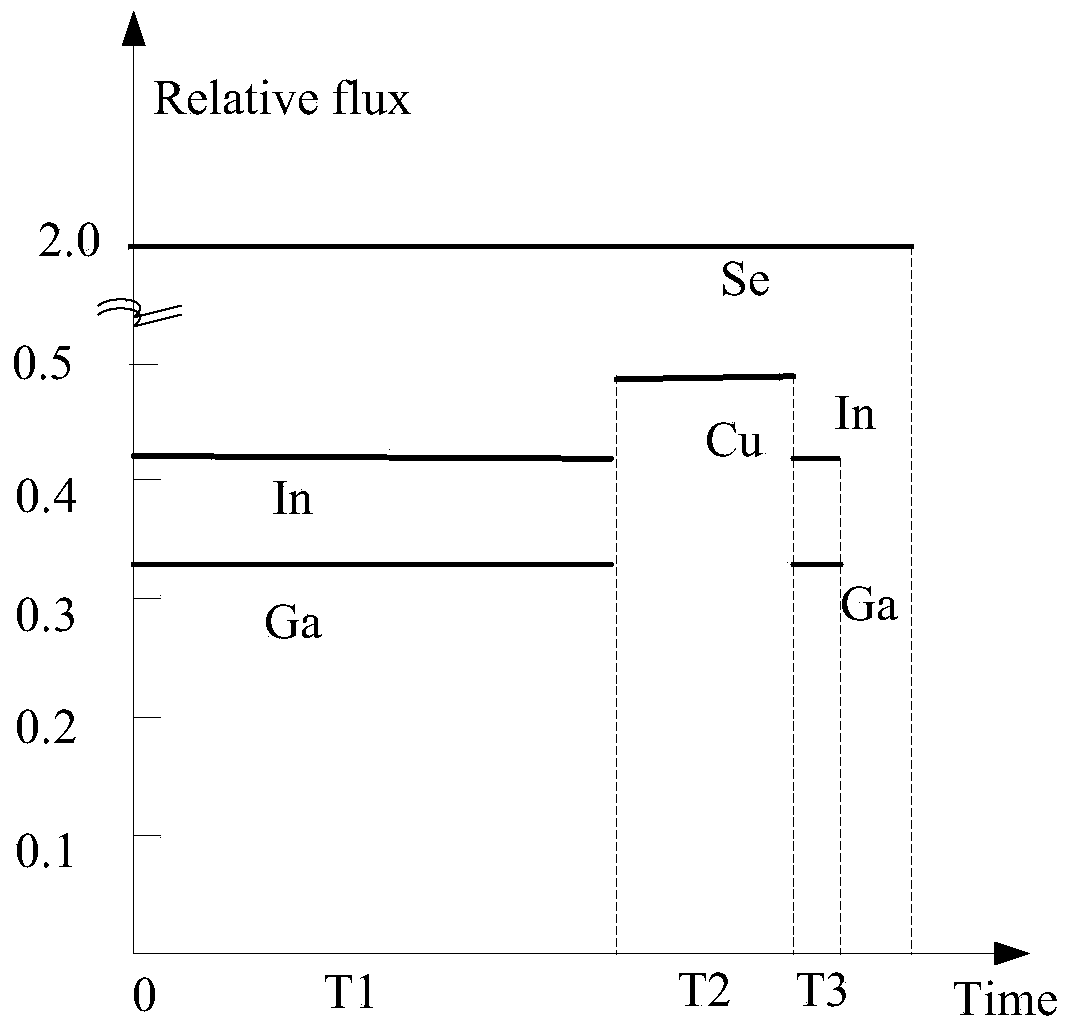
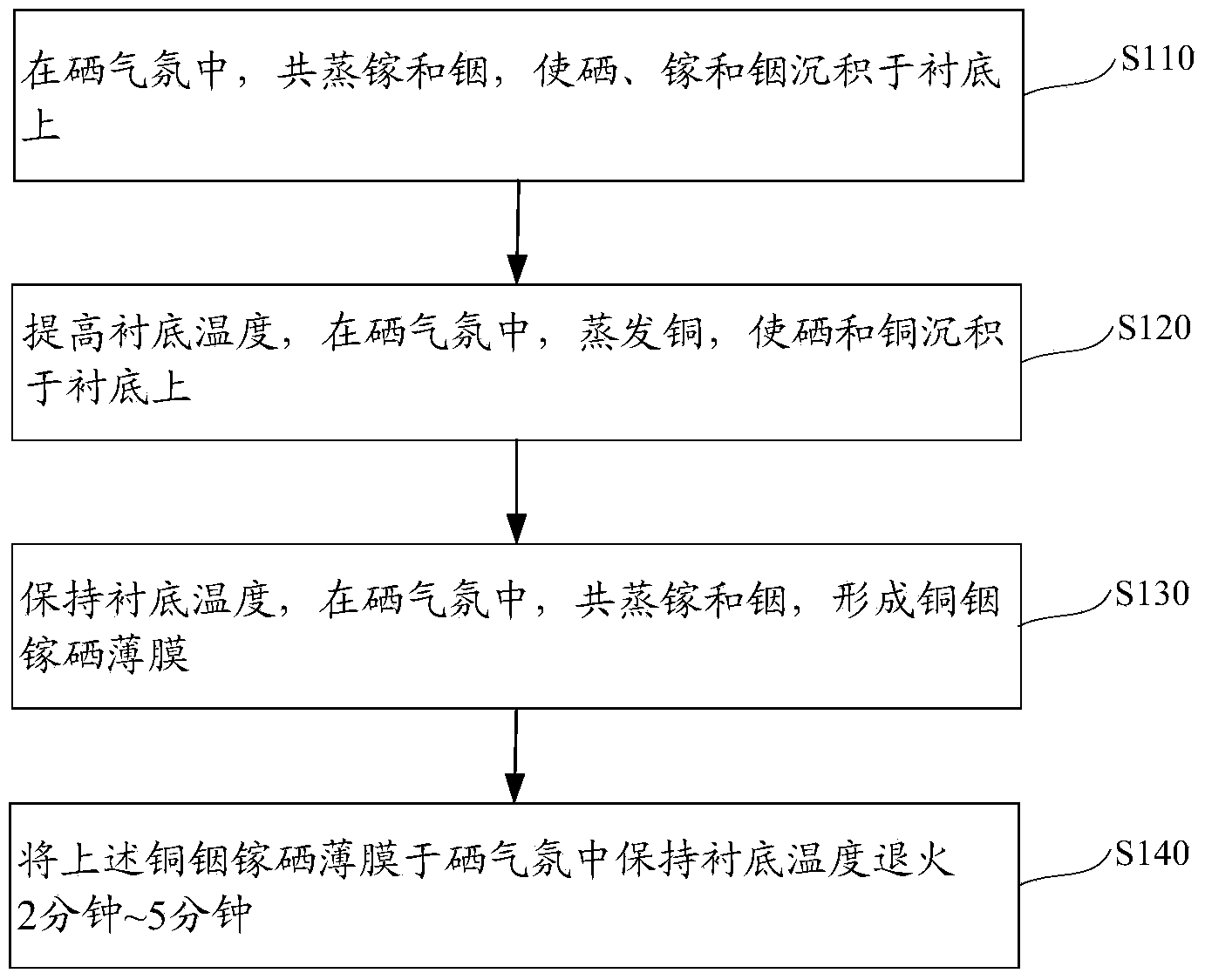
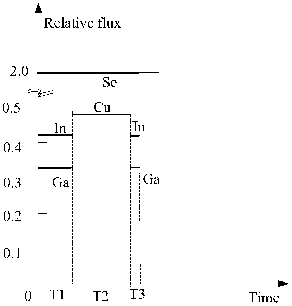
[0029] Please also see figure 2 with image 3 , the preparation method of the copper indium gallium selenide thin film of an embodiment, comprises the following steps:
[0030] Step 1 ( S110 ): in a selenium atmosphere, gallium and indium are co-evaporated, so that the selenium, gallium and indium are deposited on the substrate.
[0031] The substrate is preferably a glass substrate deposited with a back electrode layer, stainless steel foil or titanium foil, and the like.
[0032] Put the substrate and four evaporation sources of copper (Cu), indium (In), gallium (Ga) and selenium (Se) in the evaporation system, heat the substrate to the required temperature, and keep the substrate temperature constant, Selenium is evaporated to create a selenium atmosphere, gallium and indium are evaporated at the same time, and the gas atoms evaporated from the surface of the high-temperature evaporation source are deposited on the substrate with a lower temperature, so that indium, gall...
Embodiment 1
[0068] Fabrication of Copper Indium Gallium Selenium Thin Films
[0069] T1=8 minutes and 45 seconds; T3=1 minute and 15 seconds; T1:T3=7:1
[0070] 1. Step 1: Heat the soda-lime glass substrate deposited with the back electrode layer to 350°C, maintain the substrate temperature at 350°C, and evaporate selenium at the source furnace temperature of 250°C to generate a selenium atmosphere; in the selenium atmosphere Gallium and indium were co-evaporated for 8 minutes and 45 seconds (this time is denoted as T1), so that selenium, gallium and indium were deposited on the back electrode layer of the substrate, and then the evaporation of gallium and indium was stopped. The evaporation temperature of the above-mentioned gallium is 1090°C, and the evaporation rate of gallium on the substrate surface is 2.0*10 -4 pa; the evaporation temperature of indium is 970°C, and the evaporation rate of indium on the substrate surface is 6.0*10 -4 pa;
[0071] 2. Step 2: Heating the substrate ...
Embodiment 2
[0075] Fabrication of Copper Indium Gallium Selenium Thin Films
[0076] T1=8 minutes and 35 seconds; T3=1 minute and 25 seconds; T1:T3=6:1
[0077] 1. Step 1: Heating the soda-lime glass substrate deposited with the back electrode layer to 350°C, and maintaining the substrate at 350°C, evaporating selenium at 250°C to generate a selenium atmosphere, co-evaporating gallium and indium in the selenium atmosphere For 8 minutes and 35 seconds (this time is denoted as T1), selenium, gallium and indium were deposited on the back electrode layer of the substrate, and then the evaporation of gallium and indium was stopped. Among them, the evaporation temperature of gallium is 1090°C, and the evaporation rate of gallium is 2.0*10 -4 pa; the evaporation temperature of indium is 970°C, and the evaporation rate of indium is 6.0*10 -4 pa;
[0078] 2. Step 2: Heating the substrate from 350°C to 590°C within 5 minutes, and maintaining the substrate at 590°C, evaporating copper in a selenium...
PUM
 Abstract
Description
Claims
Application Information
 - R&D
- Intellectual Property
- Life Sciences
- Materials
- Tech Scout
- Unparalleled Data Quality
- Higher Quality Content
- 60% Fewer Hallucinations
Browse by: Latest US Patents, China's latest patents, Technical Efficacy Thesaurus, Application Domain, Technology Topic, Popular Technical Reports.
© 2025 PatSnap. All rights reserved.Legal|Privacy policy|Modern Slavery Act Transparency Statement|Sitemap|About US| Contact US: help@patsnap.com