Methods for manufacturing micro/nano scale pattern stamping die
A production method and pattern technology, which is applied in the field of micro-nano-scale pattern imprinting mold production, can solve the problems of unsuitable large-area nanostructure production, slow speed of high-definition graphics, and insufficient fineness of stripe scale, so as to improve the anti-counterfeiting ability , large format and low cost
- Summary
- Abstract
- Description
- Claims
- Application Information
AI Technical Summary
Problems solved by technology
Method used
Image
Examples
Embodiment 1
[0047] Embodiment 1: as image 3 As shown, the sequence includes the following steps:
[0048] (1) Electron beam lithography step;
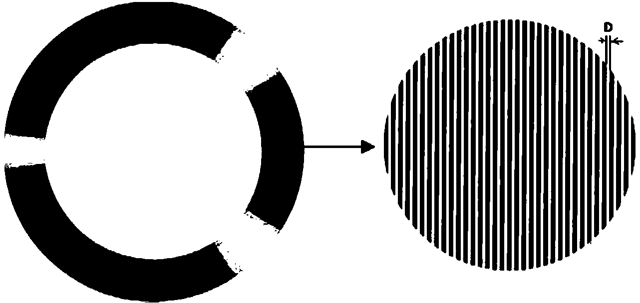
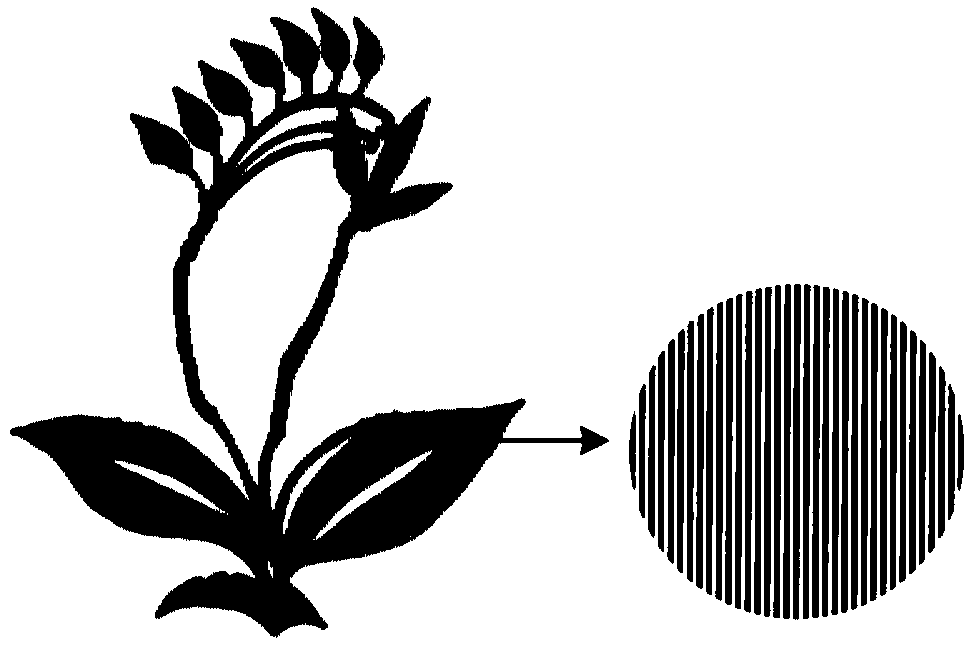
[0049] First, spin-coat ZEP520 electronic glue with a thickness of 400nm on the silicon substrate, and then use electron beam exposure to make nano-sized patterns of grating structures as shown in Figure 2(b) and Figure 2(c), develop and fix Finally, a nanometer-sized pattern with a line width of 200nm is obtained on the silicon substrate;
[0050] (2) a dry etching step;
[0051] Use the remaining electronic glue as a mask, and dry-etch the silicon substrate to obtain a nano-sized pattern with a depth of 100nm and a line width of 200nm;
[0052] (3) laser interference lithography step;
[0053] Clean and remove the remaining electronic glue, spin-coat AZ3100 photoresist with a thickness of 1500nm on the surface of the silicon substrate, and then make a photoresist on the adjacent part or surrounding part of the corresponding nanometer-sized ...
Embodiment 2
[0061] Example 2, such as Figure 4 As shown, the sequence includes the following steps:
[0062] (1) laser interference lithography step;
[0063] Spin-coat AZ3100 photoresist with a thickness of 1500nm on the surface of the silicon substrate, and then make a micro-nano-sized pattern on the photoresist as shown in Figure 2(a), and use laser interference to photoetch the micro-nano-sized pattern , after developing and fixing, a micro-nano-sized pattern with a line width of 600nm is obtained on the silicon substrate;
[0064] (2) a dry etching step;
[0065] Using the remaining photoresist as a mask, dry-etch the silicon substrate to obtain micro-nano-sized patterns with a depth of about 300nm and a line width of 600nm;
[0066] (3) Electron beam lithography step;
[0067] Clean and remove the remaining photoresist on the silicon substrate, spin-coat ZEP520 electronic glue with a thickness of 400nm on the silicon substrate, and make it on the electronic glue corresponding t...
PUM
| Property | Measurement | Unit |
|---|---|---|
| depth | aaaaa | aaaaa |
| width | aaaaa | aaaaa |
| depth | aaaaa | aaaaa |
Abstract
Description
Claims
Application Information
 - R&D
- Intellectual Property
- Life Sciences
- Materials
- Tech Scout
- Unparalleled Data Quality
- Higher Quality Content
- 60% Fewer Hallucinations
Browse by: Latest US Patents, China's latest patents, Technical Efficacy Thesaurus, Application Domain, Technology Topic, Popular Technical Reports.
© 2025 PatSnap. All rights reserved.Legal|Privacy policy|Modern Slavery Act Transparency Statement|Sitemap|About US| Contact US: help@patsnap.com


