Post-etching ashing method and forming method of magnetic sensor

A magnetic sensor and ashing technology, which is used in the manufacture/processing of electromagnetic devices, semiconductor/solid-state device manufacturing, electrical components, etc., can solve the problem of not completely removing the photoresist layer, and achieve the effect of improving the etching selectivity ratio.

Inactive Publication Date: 2014-04-16
SHANGHAI HUAHONG GRACE SEMICON MFG CORP
View PDF6 Cites 12 Cited by
  • Summary
  • Abstract
  • Description
  • Claims
  • Application Information

AI Technical Summary

Problems solved by technology

[0007] However, after the tantalum nitride layer is formed, the patterned photoresist layer cannot be completely removed by an ashing process.

Method used


Image

  • Post-etching ashing method and forming method of magnetic sensor
  • Post-etching ashing method and forming method of magnetic sensor
  • Post-etching ashing method and forming method of magnetic sensor

Examples


Embodiment Construction

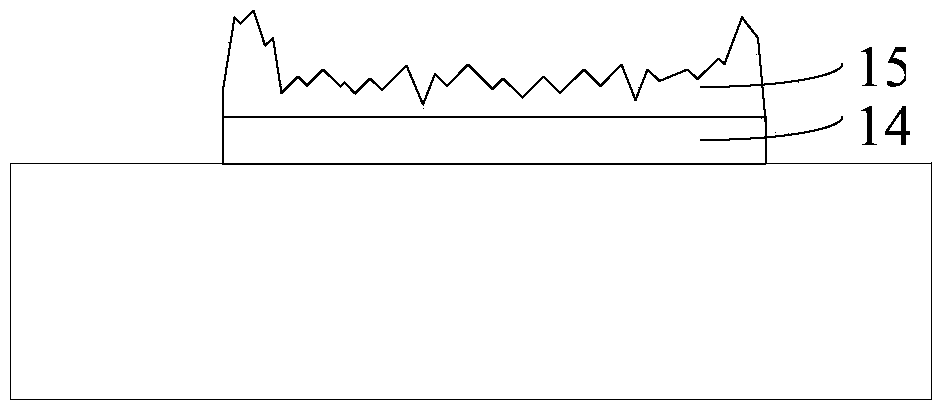
[0024] It can be known from the background art that after the tantalum nitride layer is formed, the photoresist layer used for the mask cannot be completely removed by the ashing process. Please refer to figure 1 Using the patterned photoresist layer as a mask, ashing is performed after the tantalum nitride layer 14 is formed by etching. There is still a part of the photoresist layer 15 remaining on the surface of the tantalum nitride layer 14, especially near the tantalum nitride layer 14 The remaining photoresist layer 15 at the sidewall of the layer 14 is the most. Through research on the remaining photoresist, it is found that the remaining photoresist is a polymer containing tantalum, oxygen, and carbon. This is mainly due to the fact that after part of the tantalum nitride film is etched and removed, the nitrogen The tantalum element in the tantalum oxide film will react with the photoresist to form a polymer containing tantalum, oxygen, and carbon. The polymer containing ...


PUM


Abstract

Disclosed are a post-etching ashing method and a forming method of a magnetic sensor. The post-etching ashing method comprises providing a substrate, wherein the surface of the substrate is provided with a tantalum oxide layer which is formed through etching, and the surface of the tantalum oxide layer is provided with a photoresist layer which serves as the mask for etching the tantalum oxide layer; after finishing the etching process, performing an ashing process on the photoresist layer on the surface of the tantalum oxide layer, wherein the ashing gas of the ashing process comprises oxygen and etching gas containing fluorine, the temperature range of the ashing process is smaller than or equal to 150 DEG C, and the radio frequency range of the ashing process is smaller than or equal to 500 watts. Due to the fact that the ashing gas contains the oxygen and the etching gas containing the fluorine, the photoresist layer on the surface of the tantalum oxide layer can be fully removed, and damage of the ashing process to the tantalum oxide layer and the substrate can be reduced.

Description

Technical field [0001] The invention relates to semiconductor manufacturing technology, in particular to an ashing method after etching and a method for forming a magnetic sensor. Background technique [0002] In the manufacturing process of Micro-Electro-Mechanical-Systems (MEMS) devices, tantalum nitride is a commonly used conductive material and mask material. Among them, the etching method for tantalum nitride in the prior art includes: [0003] Providing a substrate, forming a tantalum nitride film on the surface of the substrate, and forming a photoresist film on the surface of the tantalum nitride film; [0004] Exposing and developing the photoresist film to form a patterned photoresist layer; [0005] Using the patterned photoresist layer as a mask, the tantalum nitride film is etched to form a tantalum nitride layer. [0006] For more information about the etching method of tantalum nitride, please refer to the Chinese patent document with publication number CN1806325A. [00...

Claims


Application Information

Patent Timeline
Patent Type & Authority Applications(China)
IPC IPC(8): H01L21/311H01L43/12
CPCH01L21/31138H10N50/01
Inventor 张振兴奚裴熊磊
Owner SHANGHAI HUAHONG GRACE SEMICON MFG CORP
Why Eureka
Try Eureka