

Miniature PVD coat miller cutter for PCB, and making method thereof
A coating and miniature technology, applied in the direction of coating, milling cutter, milling machine equipment, etc., can solve the problems such as difficult to meet the processing requirements, achieve low friction coefficient, high hardness, and improve the service life
- Summary
- Abstract
- Description
- Claims
- Application Information
AI Technical Summary
Problems solved by technology
Method used
Image

Examples
Embodiment 1
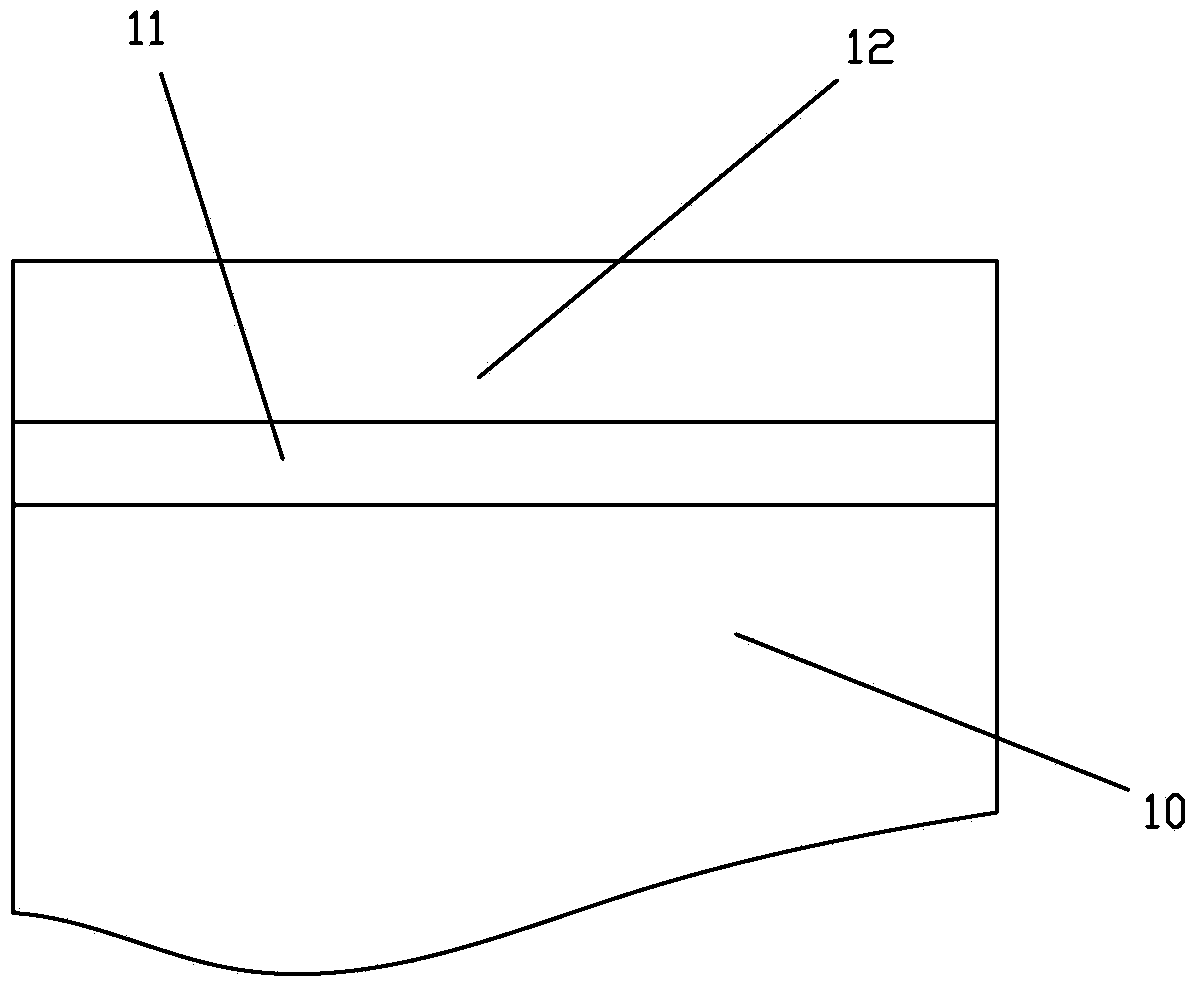
[0031] See figure 1 As shown, a PVD-coated micro-milling cutter for PCB of the present invention includes a substrate 10 and two layers of hard and wear-resistant coatings deposited on the substrate by a physical vapor deposition method; one of the coatings 11 is TiN coating, the other coating 12 is AlTiSiN coating.
[0032] MeC Coating 11 x N y O z In, Me has only one element, and x=0, z=0, y=1;
[0033] MeC Coating 12 x N y O z In, Me has three elements, and x=0, z=0, y=1.
[0034] The coating preparation method of this embodiment is as follows:
[0035] Choose a carbide PCB micro-milling cutter with a blade diameter of D1.0mm. The PCB micro-milling cutter must undergo cleaning treatments such as degreasing and cleaning. After the surface of the PCB micro-milling cutter reaches the coating standard, the coating is deposited. The first is to install the PCB milling cutter and place the PCB micro-milling cutter in the ion plating coating furnace; the second is to vacuum, turn on the ...
Embodiment 2
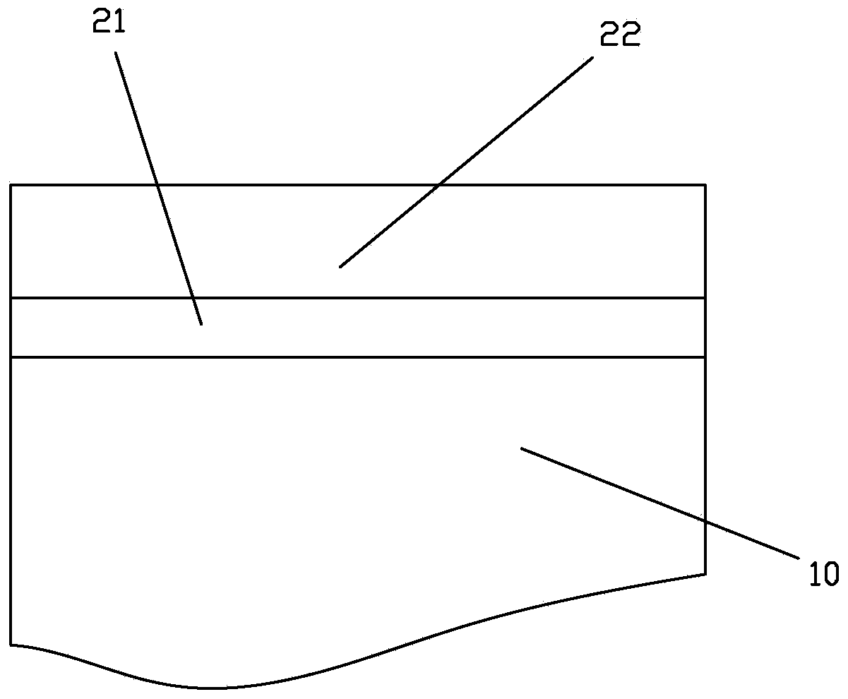
[0037] See figure 2 As shown, a PVD-coated micro-milling cutter for PCB of the present invention includes a substrate 10 and two layers of hard and wear-resistant coatings deposited on the substrate by a physical vapor deposition method; one of the coatings 21 is AlCrN coating, the other coating 22 is AlCrSiWN coating.
[0038] MeC Coating 21 x N y O z In, Me has two elements, and x=0, z=0, y=1;
[0039] MeC Coating 22 x N y O z In, Me has four elements, and x=0, z=0, y=1.
[0040] The coating preparation method of this embodiment is as follows:
[0041] A carbide PCB micro-milling cutter with a blade diameter of D1.7m is selected. The PCB micro-milling cutter must be cleaned such as degreasing and cleaning. After the surface of the PCB micro-milling cutter reaches the coating standard, the coating is deposited. The first is to install the PCB milling cutter and place the PCB micro-milling cutter in the ion plating coating furnace; the second is to vacuum, and the mechanical pump is...
Embodiment 3
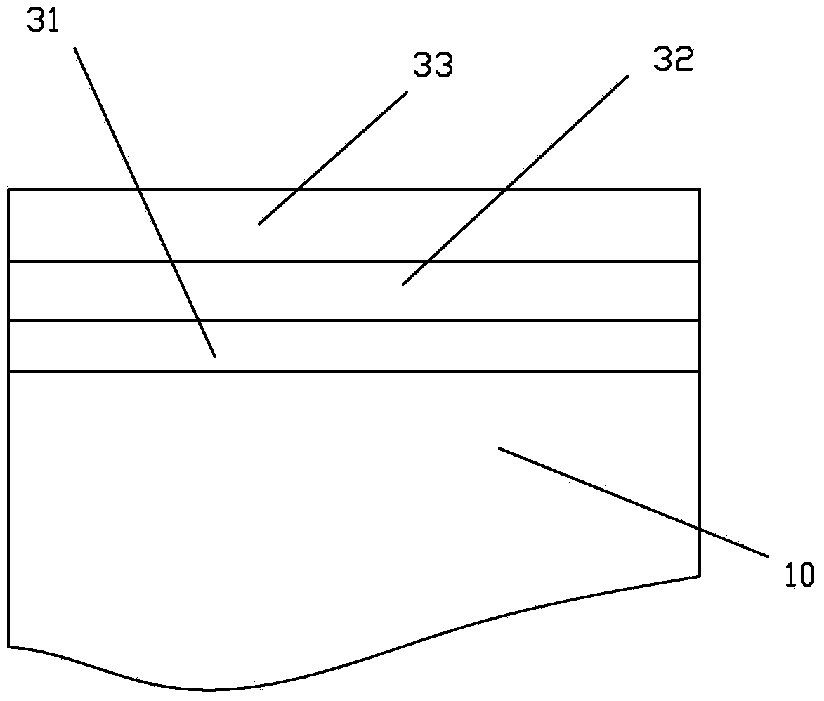
[0043] See image 3 As shown, a PVD-coated micro milling cutter for PCB of the present invention includes a substrate 10 and three layers of hard and wear-resistant coatings deposited on the substrate by a physical vapor deposition method; one of the coatings 31 is TiN coating, the other coating 32 is AlCrN coating, and the other coating 33 is AlCrTiZrNiN coating.
[0044] MeC Coating 31 x N y O z In, Me has only one element, and x=0, z=0, y=1;
[0045] MeC Coating 32 x N y O z In, Me has two elements, and x=0, z=0, y=1;
[0046] MeC Coating 33 x N y O z In, Me has five elements, and x=0, z=0, y=1.
[0047] The coating preparation method of this embodiment is as follows:
[0048] A carbide PCB micro-milling cutter with a blade diameter of D2.0mm is selected. The PCB micro-milling cutter must undergo cleaning treatments such as degreasing and cleaning. After the surface of the PCB micro-milling cutter reaches the coating standard, the coating is deposited. The first is to install the P...
PUM
| Property | Measurement | Unit |
|---|---|---|
| thickness | aaaaa | aaaaa |
| thickness | aaaaa | aaaaa |
| diameter | aaaaa | aaaaa |
Abstract
Description
Claims
Application Information