

Thin film transistor, manufacturing method for thin film transistor, array substrate and organic light-emitting display panel
A thin-film transistor and array substrate technology, applied in the display field, can solve problems such as complex process, low yield, and unsuitability for flexible substrates
- Summary
- Abstract
- Description
- Claims
- Application Information
AI Technical Summary
Problems solved by technology
Method used
Image

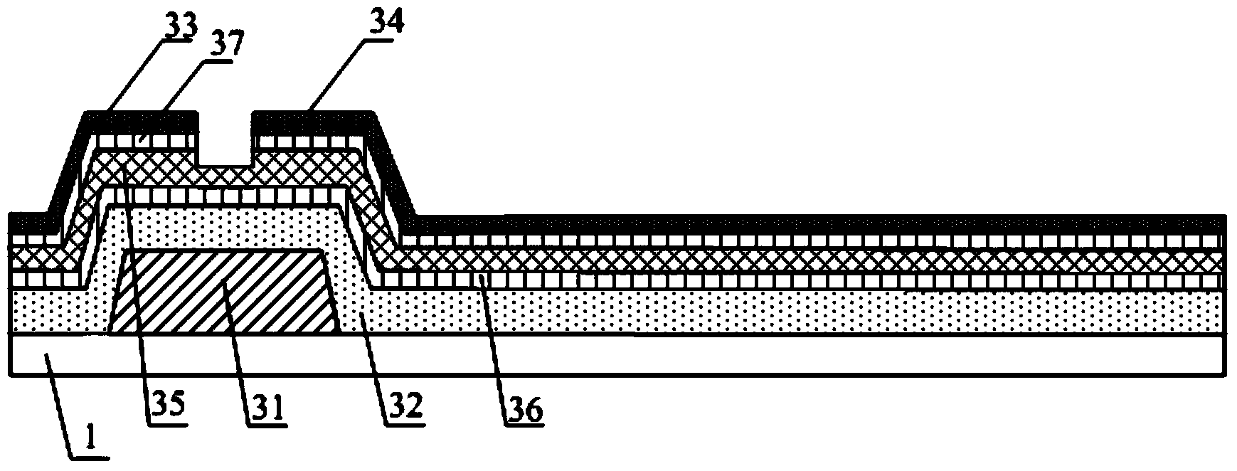


Examples
Embodiment 1
[0058] Embodiment 1: thin film transistor.
[0059] the following to figure 1 As an example, the thin film transistor provided by the embodiment of the present invention is introduced, such as figure 1 As shown, the thin film transistor includes at least an active layer 35, and also includes a first conductive layer 36 and a second conductive layer 37 located on the upper and lower sides of the active layer 35 and in contact with the active layer 35, that is to say, the active layer 35 is sandwiched between the first conductive layer 36 and the second conductive layer 37; wherein, the active layer 35 is made of carbon nanotubes with semiconductor properties or graphene materials with semiconductor properties; the first conductive layer 36 and the second conductive layer The conductive layer 37 is composed of a secondary electron emission layer having an electron multiplication function.
[0060] Of course, the TFT usually also includes a gate 31, a gate insulating layer 32 a...
Embodiment 2
[0071] Embodiment 2: array substrate.
[0072] The array substrate provided by Embodiment 2 of the present invention is similar to the prior art, and includes a substrate and a plurality of pixel units arranged in a matrix on the substrate, and each pixel unit includes at least one thin film transistor, and the thin film transistor is The thin film transistor provided in the above embodiments.
[0073] The arrangement of the thin film transistor and the organic light emitting device OLED in the organic light emitting display panel will be described below.
[0074] see figure 2 The array substrate provided by Embodiment 2 of the present invention further includes an organic light-emitting device OLED located in each pixel unit. The light-emitting layer 43 between the anodes 42, the anode 42 is connected to the drain 34 in the thin film transistor; wherein, at least one of the cathode 41 and the anode 42 is made of carbon nanotube or graphene material with conductive properti...
Embodiment 3
[0084] Embodiment 3: an organic light emitting display panel.
[0085] An embodiment of the present invention also provides an organic light emitting display panel, including the above-mentioned array substrate. The organic light-emitting display panel may be any product or component with a display function such as electronic paper, OLED panel, digital photo frame, mobile phone, and tablet computer.
[0086] In the organic light-emitting display panel provided by the embodiment of the present invention, the active layer in the thin film transistor is composed of carbon nanotubes with semiconductor properties or graphene materials with semiconductor properties, so that the carrier mobility of the semiconductor is relatively high, so that the organic light-emitting The stability of the display device is higher; at the same time, the first conductive layer and the second conductive layer are made respectively on the upper and lower sides of the active layer, and the first conduct...
PUM
| Property | Measurement | Unit |
|---|---|---|
| Thickness | aaaaa | aaaaa |
Abstract
Description
Claims
Application Information