Overlay error measurement apparatus and method

An overlay error and measuring device technology, which is applied in the field of equipment in the field of integrated circuit manufacturing, can solve the problems of limited wavelength range of measurement light, reduced information volume, small focal depth range, etc., achieve good process adaptability, reduce control difficulty, Measuring a wide range of effects

Active Publication Date: 2014-05-07
SHANGHAI MICRO ELECTRONICS EQUIP (GRP) CO LTD
View PDF7 Cites 42 Cited by
  • Summary
  • Abstract
  • Description
  • Claims
  • Application Information

AI Technical Summary

Problems solved by technology

It can be seen from its description that, first of all, the wavelength range of the measurement light used for overlay error measurement is limited in this scheme, and there may be certain process adaptability problems in the face of complex semiconductor manufacturing processes
For example, if the measurement wavelength is exactly 4 times the film thickness, the interference effect will easily occur and the reflectivity will be greatly reduced, resulting in a decrease in measurement accuracy; secondly, the large NA objective lens scheme used in this scheme has a small focal depth range
Generally speaking, in the angle-resolved spectrum measurement scheme, the effective aperture used by the measuring light is greater than 0.9, and the effective focal depth range is less than 1um if the typical measurement wavelength is 600nm. Accuracy control, which will affect the measurement speed and accuracy; if the focal plane is not well controlled, the measurement spot will easily spread out of the engraved mark under test, forming a large amount of stray light; again, this scheme can only be used to measure a single set at a time. When measuring two directions at the same time, the angle-resolved spectra of the two directions may be superimposed on each other, so the angle range contained in the angle-resolved spectrum can only be reduced, the amount of information is reduced, and the accuracy is affected.

Method used


Image

  • Overlay error measurement apparatus and method
  • Overlay error measurement apparatus and method
  • Overlay error measurement apparatus and method

Examples


Embodiment 1

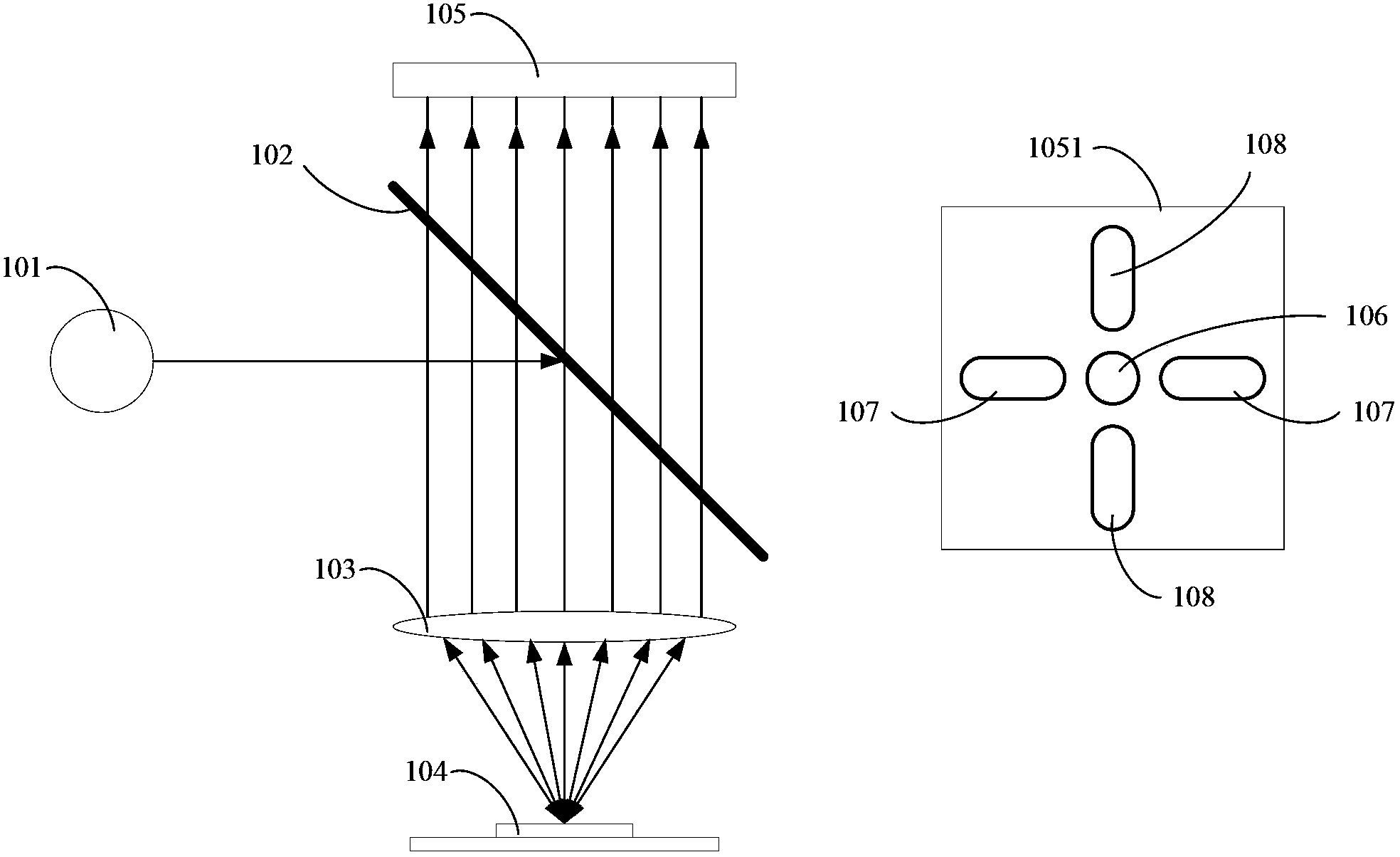
[0059] The present invention provides an overlay error measuring device, please refer to figure 1 ,include:

[0060] The broadband light source 101 is used to generate a wide-band measuring light beam. The wavelength bands of the broadband light source include visible light, ultraviolet and infrared. The broadband light source 101 can be one of a xenon lamp, a deuterium lamp and a halogen lamp or A variety of combinations, so that it can have a wider range of wavelength selection, while in the prior art, several discrete wavelengths in the visible light band are used as measurement light, and the wavelength range and selectivity are greatly limited;

[0061] A beam splitter 102, the beam splitter 102 is located on the optical path of the measurement beam emitted by the broadband light source 101, so that the measurement beam is refracted;

[0062] An objective lens 103, the objective lens 103 receives and converges the deflected measuring beam so that it is incident on the ov...

Embodiment 2

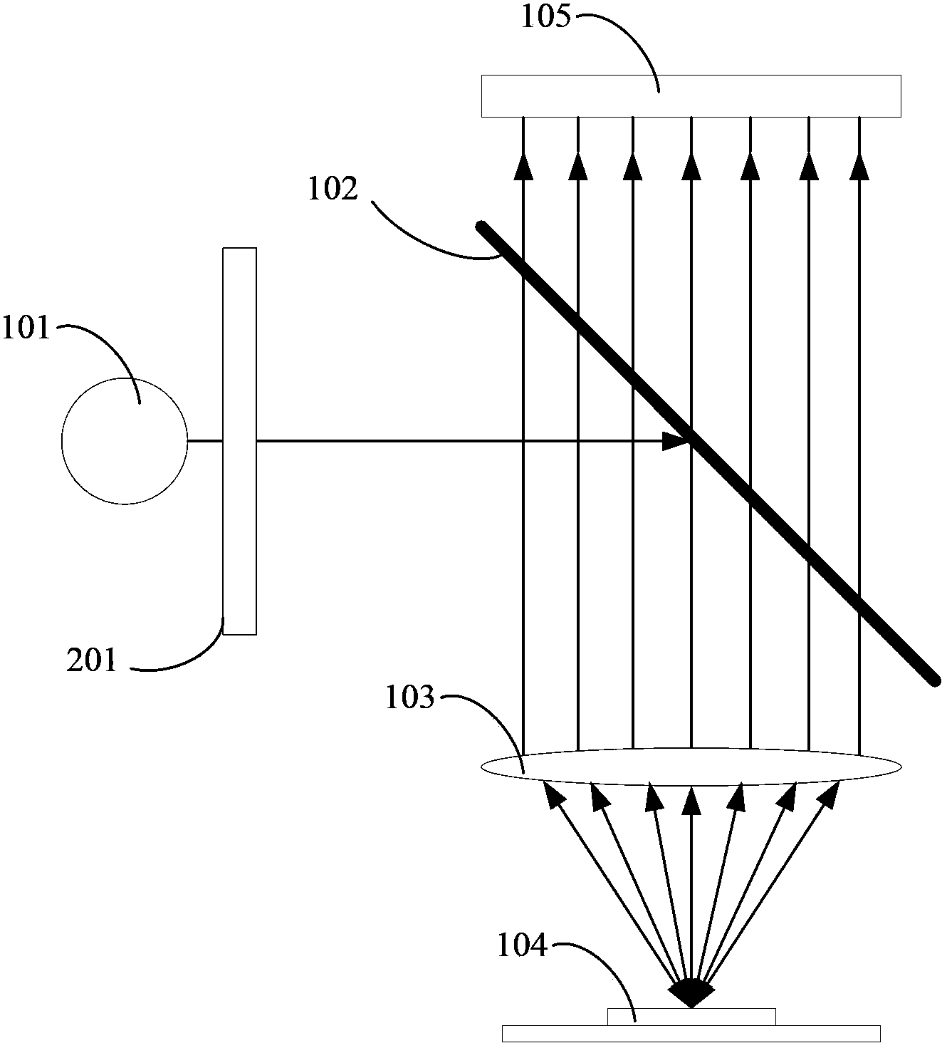
[0065] Please refer to figure 2 , in order to further improve the process adaptability and measurement accuracy of the measuring device, a polarizer 201 can be added on the basis of Embodiment 1, and the polarizer 201 can generate a polarized measurement beam. Specifically, the polarized measurement beam can be The polarization measurement beam of the TE mode may also be the polarization measurement beam of the TM mode. In different semiconductor manufacturing processes, there are certain differences in the sensitivity of different polarized lights to overlay errors. Therefore, for specific overlay measurement marks, the polarization direction with higher sensitivity can be selected for measurement to further improve process adaptability .

Embodiment 3

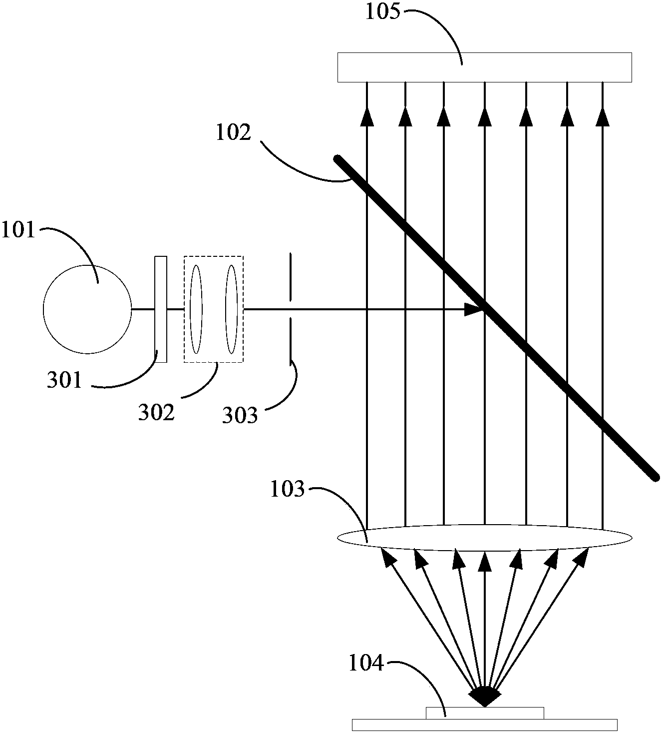
[0067] It is known that the spatial frequency of each order of diffracted light is sinθ=nλ / p, where θ is the diffraction angle, n is the diffraction order, λ is the wavelength, and p is the overlay measurement mark period. Since the measurement uses a broadband light source, within the same diffraction order, the diffracted light of each wavelength is spatially separated. In this embodiment, the overlay error is determined by measuring the light intensity asymmetry of the diffracted light of the same wavelength. Therefore, it is necessary to accurately determine the position of the diffracted light of the same wavelength on the first detector. In this embodiment, as image 3 The scheme realizes the calibration of the diffraction spectrum position: after the broadband light source 101, a filter device 301 is added, and the filter device 301 can filter out one or more wavelengths, that is, generate one or more monochromatic lights, which will be One or more separated diffractio...


PUM

PropertyMeasurementUnit
angleaaaaaaaaaa

Abstract

The invention provides an overlay error measurement apparatus and a method. According to the present invention, a wide waveband light source is adopted, the emitted wide waveband measurement light beam turns through a beam splitting prism, then is subjected to normal incidence on an overlay measurement label through an object lens, and produces diffraction, the diffraction light is received by a first detector after passing through the object lens and the beam splitting prism so as to measure the diffraction light intensity, and the asymmetry of the high-order diffraction light spectral intensity is further calculated so as to obtain the overlay error; and the adopted wide waveband has the wide measurement range, the good process adaptability is provided, and the normally-incident light beam is adopted so as to provide large depth of focus and reduce the control difficulty of the focal plane position measurement, such that the feasibility during actual measurement is increased, and the high precision measurement result can be obtained.

Description

technical field [0001] The invention relates to equipment in the field of integrated circuit manufacturing, in particular to an overlay error measurement device and method applied in photolithography measurement technology. Background technique [0002] According to the lithography measurement technology roadmap given by the International Technology Roadmap for Semiconductors (ITRS), as the critical dimension (CD) of lithography patterns enters the process node of 22nm and below, especially the double patterning (Double Patterning) technology Widely used, the measurement accuracy requirements for overlay of photolithography process parameters have entered the sub-nanometer field. Due to the limitation of imaging resolution limit, the traditional Imaging-Based overlay (IBO) technology based on imaging and image recognition has gradually been unable to meet the requirements of new process nodes for overlay measurement. Diffraction-Based overlay (DBO) is gradually becoming the...

Claims


Application Information

Patent Timeline
Patent Type & Authority Applications(China)
IPC IPC(8): G03F7/20G03F9/00
Inventor 陆海亮王帆
Owner SHANGHAI MICRO ELECTRONICS EQUIP (GRP) CO LTD
Why Eureka
Try Eureka