Supercharge Your Innovation With Domain-Expert AI Agents!

Method for manufacturing polysilicon resistor in metal wolfram silicide gate electrode technology

A polysilicon resistor and metal silicidation technology, which is applied in the manufacture of semiconductor/solid state devices, circuits, electrical components, etc., can solve the problems affecting the resistance accuracy, limiting the application range of polysilicon resistors, and the proportion of contact hole resistance fluctuations. Contact hole resistance, improved in-plane uniformity, and reduced ripple effects

Active Publication Date: 2014-05-07
SHANGHAI HUAHONG GRACE SEMICON MFG CORP
View PDF5 Cites 4 Cited by
  • Summary
  • Abstract
  • Description
  • Claims
  • Application Information

AI Technical Summary

Problems solved by technology

However, when the polysilicon resistance is small (such as several square resistances), the fluctuation of the contact hole resistance accounts for a large proportion, which seriously affects the precision of the resistance and limits the application range of this type of polysilicon resistance.

Method used


Image

  • Method for manufacturing polysilicon resistor in metal wolfram silicide gate electrode technology
  • Method for manufacturing polysilicon resistor in metal wolfram silicide gate electrode technology
  • Method for manufacturing polysilicon resistor in metal wolfram silicide gate electrode technology

Examples


Embodiment Construction

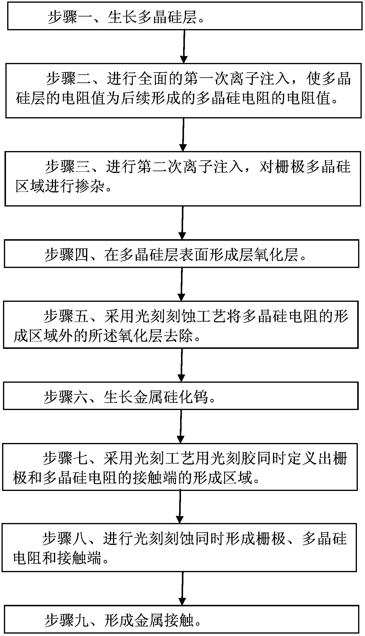
[0028] Such as image 3 Shown is the flow chart of the manufacturing method of the polysilicon resistance in the metal tungsten silicide gate process of the embodiment of the present invention; Figure 4A to Figure 4E Shown is a schematic cross-sectional view of the device in each step of the method of the embodiment of the present invention. The method for manufacturing polysilicon resistors in the metal silicide gate process of the embodiment of the present invention includes the following steps:

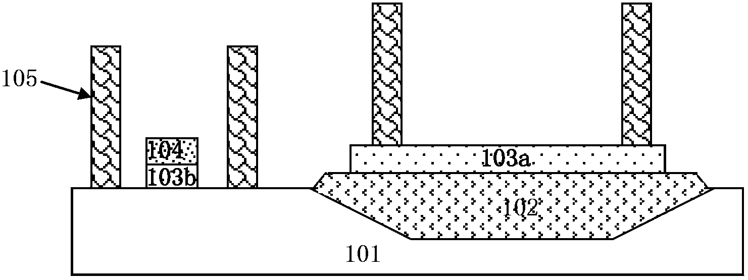
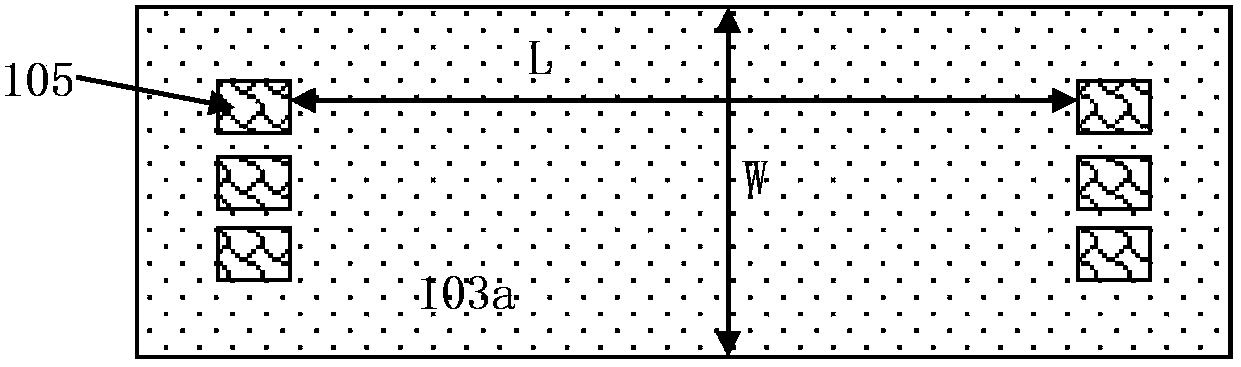
[0029] Step 1, such as Figure 4A As shown, a field oxide layer 2 is formed on a semiconductor substrate such as a silicon substrate 1. The field oxide layer 2 can be a shallow trench isolation oxide layer or a local field oxide layer, and the field oxide layer 2 isolates an active region. A polysilicon layer 3 is grown on a semiconductor substrate 1 .

[0030] Step two, such as Figure 4A As shown, a comprehensive first ion implantation is performed on the front side of the s...


PUM


Abstract

The invention discloses a method for manufacturing a polysilicon resistor in metal wolfram silicide gate electrode technology. The method comprises steps of: growing a polysilicon layer; carrying out comprehensive first ion implantation in order to make the resistance value of the polysilicon layer as the resistance value of the polysilicon resistor formed subsequently; using second ion implantation technology to dope the polysilicon layer in the forming area of the gate polysilicon; forming an oxide layer on the surface of the polysilicon layer; removing the oxide layer outside the forming area of the polysilicon resistor by using photoetching technology; growing metal wolfram silicide; simultaneously defining the forming area of a contact end of a gate electrode and the polysilicon resistor by using photoetching technology and photoresist; successively etching the metal wolfram silicide and the polysilicon layer by using the photoresist as a mask and simultaneously forming a gate electrode, the polysilicon resistor, and the contact end; and forming a metal contact hole. The method may decrease the resistance of the contact hole of the polysilicon resistor, improve the in-plane uniformity of the polysilicon resistor, and increase the precision of the polysilicon resistor.

Description

technical field [0001] The invention relates to a semiconductor integrated circuit manufacturing process method, in particular to a polysilicon resistor manufacturing method in the metal tungsten silicide gate process. Background technique [0002] In the process of polycide, metal tungsten silicide (WSi) grown on polysilicon is generally used as the gate of MOS devices such as LDMOS (Laterally Diffused Metal Oxide Semiconductor) devices. In the process of polycide (polycide) such as metal tungsten silicide gate, high-resistance polysilicon resistance (HRP) is a very necessary optional process, and in some processes, the polysilicon of the gate and the polysilicon of the polysilicon resistance are formed by simultaneous deposition. . Such as figure 1 As shown, it is a schematic cross-sectional view of a polysilicon resistor formed in a polysilicon resistor manufacturing method in an existing metal tungsten silicide gate process; first, a field oxygen layer 102 is formed on...

Claims


Application Information

Patent Timeline
Patent Type & Authority Applications(China)
IPC IPC(8): H01L21/28
CPCH01L21/28061H01L21/76897H01L29/401H01L2221/1068
Inventor 陈瑜赵阶喜罗啸
Owner SHANGHAI HUAHONG GRACE SEMICON MFG CORP
Features
  • R&D
  • Intellectual Property
  • Life Sciences
  • Materials
  • Tech Scout
  • Unparalleled Data Quality
  • Higher Quality Content
  • 60% Fewer Hallucinations
Learn More