Preparation method for needle point type silicon nanowire

A silicon nanowire and needle-tip technology, which is applied in the field of preparation of needle-point silicon nanowires, can solve the problems of incapable of large-scale industrial production, general poor adaptability of the method, disordered nanowires, etc., and achieves the convenience of large-scale industrial production and good chemical stability sex, method and reliable effect

Active Publication Date: 2014-05-14
西安艾斯达特新材料科技有限公司
View PDF2 Cites 7 Cited by
  • Summary
  • Abstract
  • Description
  • Claims
  • Application Information

AI Technical Summary

Problems solved by technology

Although these methods can control the structure and morphology of the grown nanowires, the methods generally have poor adaptability, cannot be mass-

Method used


Image

  • Preparation method for needle point type silicon nanowire
  • Preparation method for needle point type silicon nanowire
  • Preparation method for needle point type silicon nanowire

Examples


Embodiment Construction

[0034] The present invention will be described in detail below in conjunction with the accompanying drawings and embodiments.

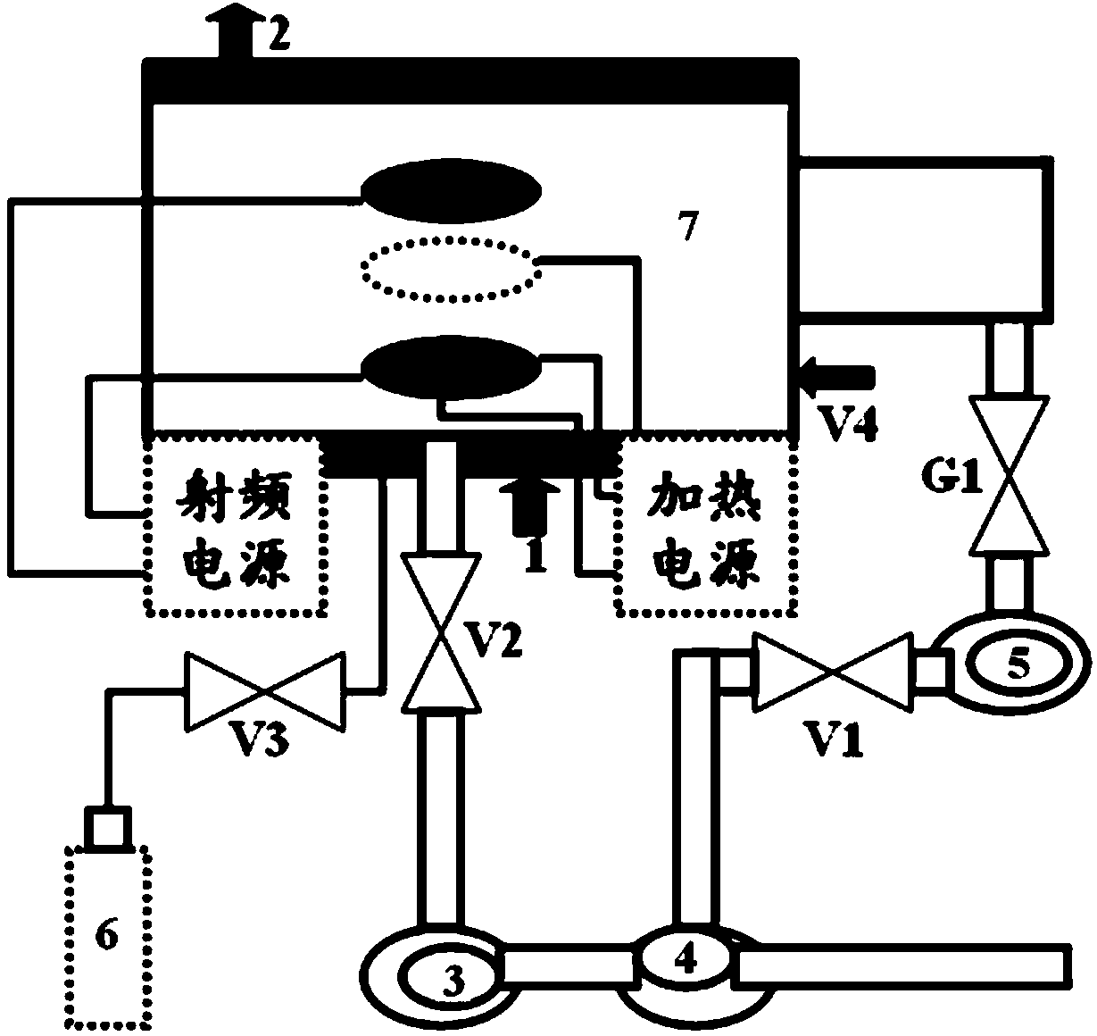
[0035] The invention provides a method for preparing acicular silicon nanowires by using plasma enhanced chemical vapor deposition (PECVD) technology and using silane as a reaction precursor.

[0036] The invention adopts the most suitable gas-liquid-solid mechanism for growing nanowires, reduces the reaction temperature through plasma enhancement, and increases the growth speed of nanowires. The Au film is deposited on the substrate by ion sputtering, and the shape of the needle-shaped nanowires is controlled by the consumption and size change of the alloy droplets after annealing. This method has high reliability, is convenient for industrial production, and can effectively control the needle tip of silicon nanowires. growth.

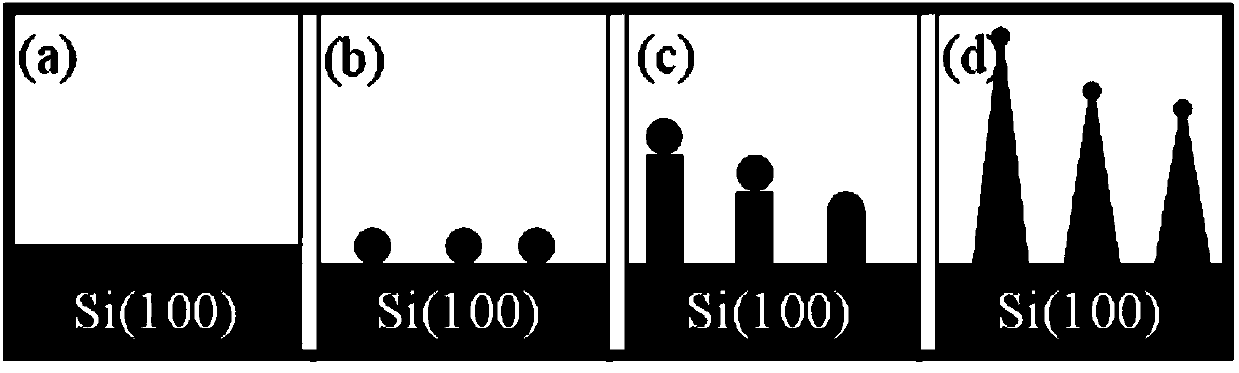
[0037] see figure 2 , the Au film deposited by sputtering on the silicon substrate in the present invention will form go...


PUM


Abstract

The invention provides a preparation method for a needle point type silicon nanowire. The preparation method comprises the following steps: depositing an Au thin film with the thickness of 5-10nm on a cleanly-washed substrate; transferring the substrate deposited with the Au film to a PECVD (Plasma Enhanced Chemical Vapor Deposition) reaction cavity; heating to 800 DEG C within 30 minutes and annealing for 40 minutes; introducing 40sccm of silane and maintaining a reaction pressure to 32pa so as to carry out a luminance build-up reaction; continuously reacting for 1 hour at 600-800 DEG C; annealing the Au film which is sputtered and deposited on the substrate to form silicon alloy liquid drops which are used as a growth catalyst of the needle point type silicon nanowire; after a silicon source in a gas phase is saturated in the alloy liquid drops, gradually separating out the silicon nanowire to grow. The dispersion of gold in the alloy liquid drops enables the volume to be gradually reduced so that the diameter of the catalytically-growing nanowire is reduced along the length direction to form a needle point shape. The preparation method is simple in process and is convenient for large-area growth; the prepared needle point type silicon nanowire can be widely applied to fields of SERS (Surface Enhanced Raman Scattering) and the like.

Description

technical field [0001] The invention relates to a method for preparing needle-point silicon nanowires. Background technique [0002] In 1974, when Fleishmann et al. studied the Raman spectrum of pyridine molecules adsorbed on silver electrodes, they found that the intensity of their spectral lines was significantly enhanced and named it Surface Enhanced Raman Scattering (SurfaceEnhancedRamanScattering). Surface-enhanced Raman scattering (SERS) is a highly sensitive and high-resolution analytical technique that has received great attention since its discovery. The key to SERS research lies in the preparation of substrates with excellent performance, which requires a high enhancement factor, good uniformity and repeatability, and low cost. Utilizing the excellent properties of one-dimensional semiconductor nanowires, such as good processability and large specific surface area, gold and silver particles that produce Raman-enhanced activity can be conveniently modified on the s...

Claims


Application Information

Patent Timeline
IPC IPC(8): C01B33/027C23C16/24B82Y30/00B82Y40/00
Inventor 马大衍黄剑马飞宋忠孝徐可为
Owner 西安艾斯达特新材料科技有限公司
Why Eureka
Try Eureka